A Circuit for Improving the Waveform and Modulation Depth of Non-contact Card Strong Field Modulation

A modulation waveform, non-contact card technology, applied to record carriers, instruments, computer parts, etc. used in machines, can solve the problems of unsatisfactory modulation waveform, shallow modulation depth of strong field, and large area of ​​modulation discharge devices.

Active Publication Date: 2017-10-31
BEIJING CEC HUADA ELECTRONIC DESIGN CO LTD
View PDF3 Cites 0 Cited by
  • Summary
  • Abstract
  • Description
  • Claims
  • Application Information

AI Technical Summary

Problems solved by technology

[0003] The purpose of the present invention is to solve the problems that the modulation depth of the strong field is too shallow, the modulation waveform is not ideal and the area of ​​the modulation discharge device is too large, and provide a method that does not increase the area of ​​the modulation discharge device additionally, but also increases the depth of the strong field modulation, improving Modulation Waveform Scheme

Method used


Image

  • A Circuit for Improving the Waveform and Modulation Depth of Non-contact Card Strong Field Modulation
  • A Circuit for Improving the Waveform and Modulation Depth of Non-contact Card Strong Field Modulation

Examples


Embodiment Construction

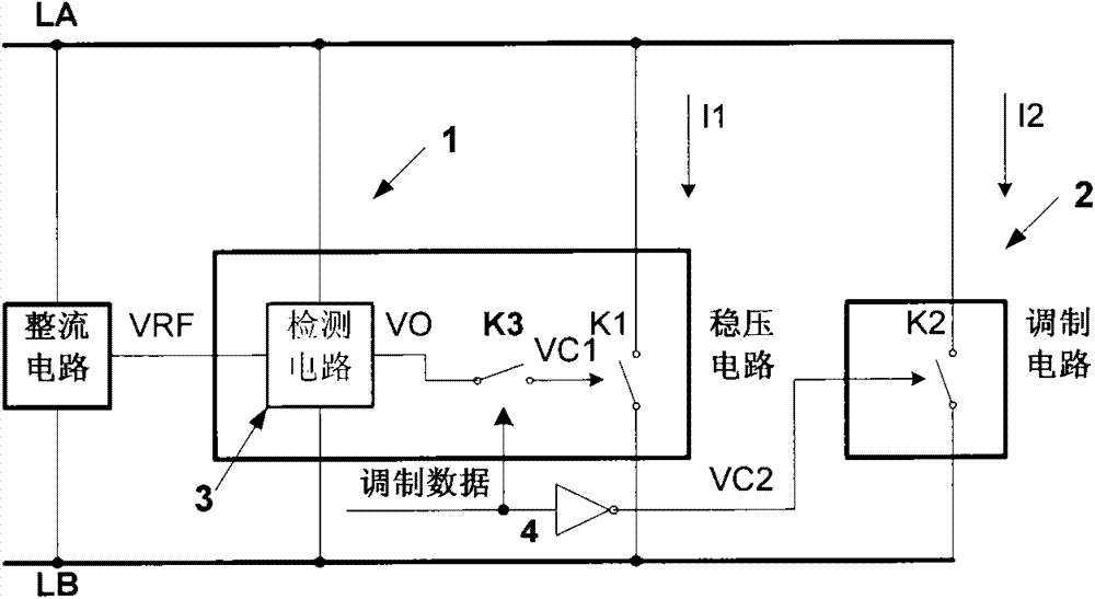
[0015] The invention proposes a circuit for improving the modulation waveform and modulation depth of the non-contact card strong field. The circuit comprises: a voltage stabilizing circuit (1), a modulating circuit (2) and an inverter (4).

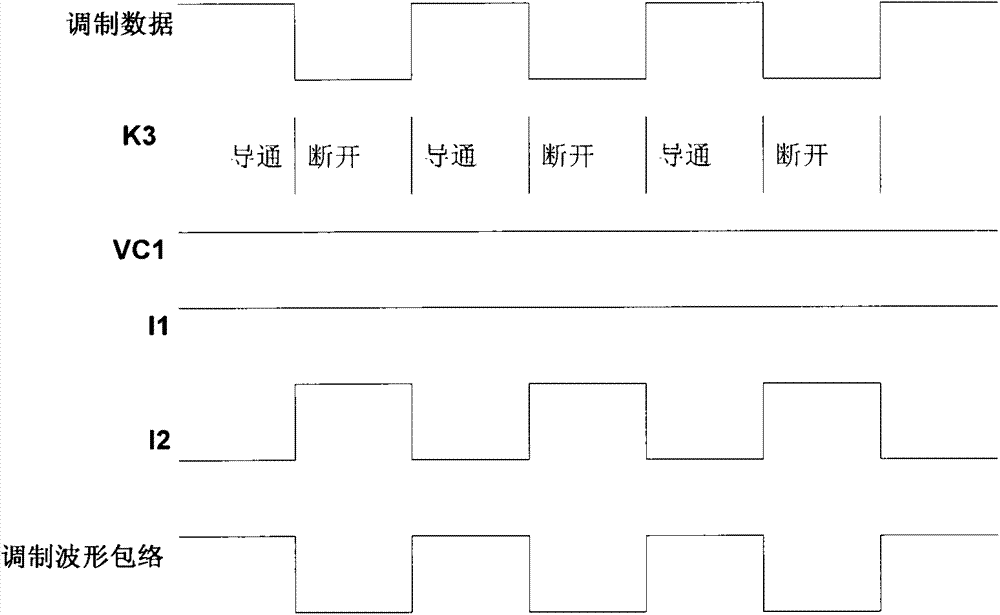
[0016] In the voltage stabilizing circuit, there is a switch K3 between the output VO of the detection circuit and the control terminal VC1 of the discharge switch K1, and the on and off of the switch K3 is controlled by the modulation data. The switch K3 is turned off in the modulation phase, and the switch K3 is turned on in the non-modulation phase. The switch K3 can be implemented with NMOS or PMOS, and can also be implemented with a transmission gate. The switch K1 can be implemented in the form of a MOS tube, or replaced by two switches connected between the antenna signal LA, the ground and the antenna signal LB, and the ground, or replaced by a switch connected between the RF power supply and the ground .

[0017] The modulation...


PUM


Abstract

The invention proposes a circuit for improving the modulation waveform and modulation depth of the non-contact card strong field, which can obtain better modulation waveform and modulation depth in the strong field without changing other circuits.

Description

technical field [0001] The present invention relates to a voltage stabilizing circuit and a modulating circuit of a non-contact card chip, and more specifically, the present invention relates to a circuit for improving the modulation waveform and modulation depth of a non-contact card strong field. Background technique [0002] There are two parts of the discharge circuit inside the contactless card chip: the discharge circuit of the voltage stabilizing circuit and the discharge circuit of the modulation circuit. The discharge current of the voltage stabilizing circuit is related to the antenna voltage and the RF power supply voltage. When it is detected that the antenna and RF power supply are lowered, the discharging current of the voltage stabilizing circuit decreases. When the card sends data to the card reader, the modulation circuit starts to discharge current, causing the amplitude of the card antenna to drop. When the voltage regulator circuit detects this drop, it ...

Claims


Application Information

Patent Timeline
Patent Type & Authority Patents(China)
IPC IPC(8): G06K19/077
Inventor 刘晓艳马哲
Owner BEIJING CEC HUADA ELECTRONIC DESIGN CO LTD
Why Eureka
Try Eureka