Electro-absorption optical modulator integrated with a laser to produce high speed, uncooled, long distance, low power, 1550 nm optical communication device with optimized parameters

a technology of electromagnetic absorption and optical modulator, which is applied in the direction of semiconductor lasers, instruments, optics, etc., can solve the problems of difficult to achieve long distance transmission for a distance of 40 km or more by uncooled operation, and the method is not suitable for the 1550 nm band of signal light wavelength

Active Publication Date: 2010-10-05
LUMENTUM JAPAN INC
View PDF7 Cites 2 Cited by
  • Summary
  • Abstract
  • Description
  • Claims
  • Application Information

AI Technical Summary

Benefits of technology

[0023]The present invention provides a light emission device using an EA modulator having optimal detuning in the 1550 nm band and a quantum well structure suitable for a long distance optical communication for a distance of 40 km or more, thereby providing an inexpensive light source.
[0024]For the operation of the EA / DFB laser in the 1550 nm band of the signal light wavelength, trade off between the chirping and the extinction ratio needs to be considered. This is because the amount of the dispersion during fiber transmission in the 1300 nm band of the signal light wavelength is substantially zero, while the fiber dispersion is as large as about 20 ps / nm / km in the 1550 nm band. For the setting of the detuning assuming the uncooled operation, when the temperature becomes lower, the detuning becomes larger. The larger detuning is, the higher voltage is required for controlling the detuning to an appropriate detuning. In this case, the slanting of the band increases to decrease the confinement effect of carriers in the quantum well. As a result, a spatial overlap of the wave functions of electrons and holes is decreased to deteriorate the extinction ratio.
[0026]In the conventional EA / DFB laser, a multi-quantum well at least including In, Ga, As, and P is generally used as the optical absorption layer. In the InGaAsP system quantum well described above, the trade off between the chirping and the extinction ratio is severe, as described above. The long distance transmission for a distance of 40 km or more by the uncooled operation is difficult to be attained. This is due to the feature in which, in the band structure of the InGaAsP material system, the energy band offset between the quantum well layer and the barrier layer is smaller on the side of the conduction band and larger on the side of the valance band. On the contrary, the quantum well structure in which the well layer is made of InGaAlAs, InGaAsP, or InGaAs, and the barrier layer is made of InGaAlAs or InAlAs has excellent features as described below and can be said suitable as an optical absorption layer of the EA modulation device aiming at an uncooled operation.
[0027](1) The band offset on the side of the conduction band is large and the leakage of the wave function to the outside of the quantum well is small in the quantum well structure. Thus, a spatial overlap of wave functions of electrons and holes is large, and the extinction ratio is improved.
[0028](2) The energy band offset between the quantum well and the barrier layer is smaller on the side of the valence band than on the side of the conduction band. Holes are hardly accumulated in the quantum well. Thus, since this is suitable for a high speed modulation operation and chirping during modulation is suppressed, this is advantageous for long distance transmission.

Problems solved by technology

However, using the methods described above means to increase chirping.
The methods are not suitable for the operation in the 1550 nm band of the signal light wavelength.
The long distance transmission for a distance of 40 km or more by the uncooled operation is difficult to be attained.

Method used


Image

  • Electro-absorption optical modulator integrated with a laser to produce high speed, uncooled, long distance, low power, 1550 nm optical communication device with optimized parameters
  • Electro-absorption optical modulator integrated with a laser to produce high speed, uncooled, long distance, low power, 1550 nm optical communication device with optimized parameters
  • Electro-absorption optical modulator integrated with a laser to produce high speed, uncooled, long distance, low power, 1550 nm optical communication device with optimized parameters

Examples


embodiment 1

RWG-EA / DFB (DBR)

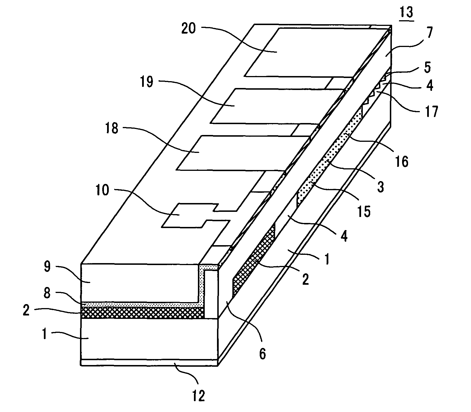
[0054]A process for manufacturing a semiconductor optical integrated device according to Embodiment 1 of the present invention is described with reference to FIG. 5 and FIG. 6. The drawings are only for the purpose of explaining the embodiment. The size and scale of the drawings showing the embodiment are not necessarily identical.

[0055]At first, a quantum well structure 2 made of an InGaAlAs system is formed on an n-InP substrate 1 as an electro-absorption optical modulator using an MOCVD method (FIG. 5A). In this case, a light emission wavelength of the quantum well structure at a temperature of 25° C. is about 1470 nm. For example, a desired light emission wavelength can be obtained by laminating a quantum well layer with a thickness of 6 nm and with a compositional ratio of In, Ga, and Al at 0.54:0.38:0.08, and a barrier layer with a thickness of 10 nm and with a compositional ratio of In, Ga, and Al at 0.52:0.33:0.15. Further, an optical confinement structure su...

embodiment 2

BH-EA / DFB (DBR)

[0070]FIG. 7A is a perspective view illustrating a construction according to another embodiment of a semiconductor optical integrated device applied with the present invention. FIG. 7B is a perspective view illustrating a cross section cut along a central line. However, the drawing is only for explaining this embodiment and the size and scale of the drawing showing this embodiment are not necessarily identical.

[0071]At first, a quantum well structure 2 made of an InGaAlAs system is formed on an n-InP substrate 1 as an electro-absorption optical modulator using an MOCVD method. In this case, a light emission wavelength of the quantum well structure 2 at a temperature of 25° C. is about 1470 nm. For example, a desired light emission wavelength can be obtained by laminating a quantum well layer with a thickness of 6 nm and with a compositional ratio of In, Ga, and Al at 0.54:0.38:0.08, and a barrier layer with a thickness of 10 nm and with a compositional ratio of In, Ga...

embodiment 3

RWG-EA / Variable Wavelength LD

[0085]FIG. 8A is a perspective view showing the constitution according to another embodiment of a semiconductor optical integrated device formed as a variable wavelength LD applied to the present invention. FIG. 8B is a perspective view illustrating a cross section cut along a central line. Figures for the processes shown in FIGS. 5 and 6 in Embodiment 1 are not illustrated. However, the drawing is only for the explanation of this embodiment and the size and scale of the drawing showing this embodiment are not necessarily identical.

[0086]A quantum well structure 2 made of an InGaAlAs system is formed on an n-InP substrate 1 as an electro-absorption optical modulator using an MOCVD method. In this case, a light emission wavelength of the quantum well structure at a temperature of 25° C. is about 1470 nm. For example, a desired light emission wavelength can be obtained by forming a quantum well layer with a thickness of 6 nm and with a compositional ratio ...


PUM


Abstract

In a conventional EA / DFB laser, since the temperature dependence of the operation wavelength of the EA portion is substantially different from that of the DFB portion, the temperature range over which a stable operation is possible is small. In the case of using the EA / DFB laser as a light emission device, an uncooled operation is not possible. An EA / DFB laser which does not require a temperature control mechanism is proposed.A quantum well structure in which a well layer made of any one of InGaAlAs, InGaAsP, and InGaAs, and a barrier layer made of either one of InGaAlAs or InAlAs is used for an optical absorption layer of an EA modulator. By properly determining detuning at a temperature of 25° C. and a composition wavelength of the barrier layer in the quantum well structure used for the optical absorption layer, it can be realized to suppress the insertion loss, maintain the extinction ratio, and reduce chirping simultaneously over a wide temperature range from −5° C. to 80° C.

Description

CLAIM OF PRIORITY[0001]The present invention application claims priority from Japanese application JP 2006-105932 filed on Apr. 7, 2006 the content of which is hereby incorporated by reference into this application.FIELD OF THE INVENTION[0002]The present invention relates to a semiconductor optical modulation device and an integrated semiconductor light emission device integrating the same.BACKGROUND OF THE INVENTION[0003]With the proliferation of broad band networks, the trend of increasing the communication speed to 10 Gbit / s or higher has been accelerated in metropolitan optical communication networks connecting cities and relay stations. In the metropolitan optical communication networks, a fiber transmission distance of 40 to 80 km has been demanded for long distance transmission. In an optical communication system for the metropolitan optical communication network, it is an important subject to reduce the size and the power consumption of the optical transmitter / receiver modul...

Claims


Application Information

Patent Timeline
Patent Type & Authority Patents(United States)
IPC IPC(8): H01S3/04H01S5/00
CPCB82Y20/00G02F1/01708H01S5/0265G02F2001/0157G02F1/0157
Inventor MAKINO, SHIGEKI
Owner LUMENTUM JAPAN INC
Why Eureka
Try Eureka