Semiconductor device

a technology of semiconductor devices and short channels, applied in semiconductor devices, semiconductor/solid-state device details, electrical apparatus, etc., can solve the problems of reducing the total performance of an integrated circuit, increasing power consumption, and extremely difficult to suppress the short channel effect, so as to reduce the effect of suppressing the short channel effect and fluctuation in the threshold

Active Publication Date: 2010-08-12
SONY CORP
View PDF8 Cites 211 Cited by
  • Summary
  • Abstract
  • Description
  • Claims
  • Application Information

AI Technical Summary

Benefits of technology

[0008]In the case where the p-type MOS transistor and the n-type MOS transistor are adjacent to each other as described above, for the purpose of suppressing the short channel effect, it is considered to form both of the transistors in the SOI and provide both of the transistors with back gates. In relation with the threshold of a gate voltage, it is necessary to use an n-type impurity layer as the back gate of the p-type MOS transistor, apply positive voltage to the n-type impurity layer, use a p-type impurity layer as the back gate of the n-type MOS transistor, and apply negative voltage to the p-type impurity layer. However, in this case, current easily flows between the back gate of the p-type MOS transistor and the back gate of the n-type MOS transistor. When the current (leak current) value increases, the voltage of the back gate drops more than a desired value. In the case where the voltage drop in the back gate varies among the transistors, the characteristics of the transistors vary among the transistors. When the voltage of the back gate drops (becomes close to zero volt), the threshold decreases, and the effect of suppressing the short channel effect decreases.
[0009]It is therefore desirable to provide a semiconductor device capable of suppressing both the short channel effect and fluctuation in the threshold.

Problems solved by technology

However, power consumption also increases, and a phenomenon that total performance of an integrated circuit becomes lower than that of an existing integrated circuit is conspicuous.
Consequently, when MOS transistors are formed in bulk silicon crystal, it is extremely difficult to suppress the short channel effect.

Method used


Image

  • Semiconductor device
  • Semiconductor device
  • Semiconductor device

Examples


embodiment

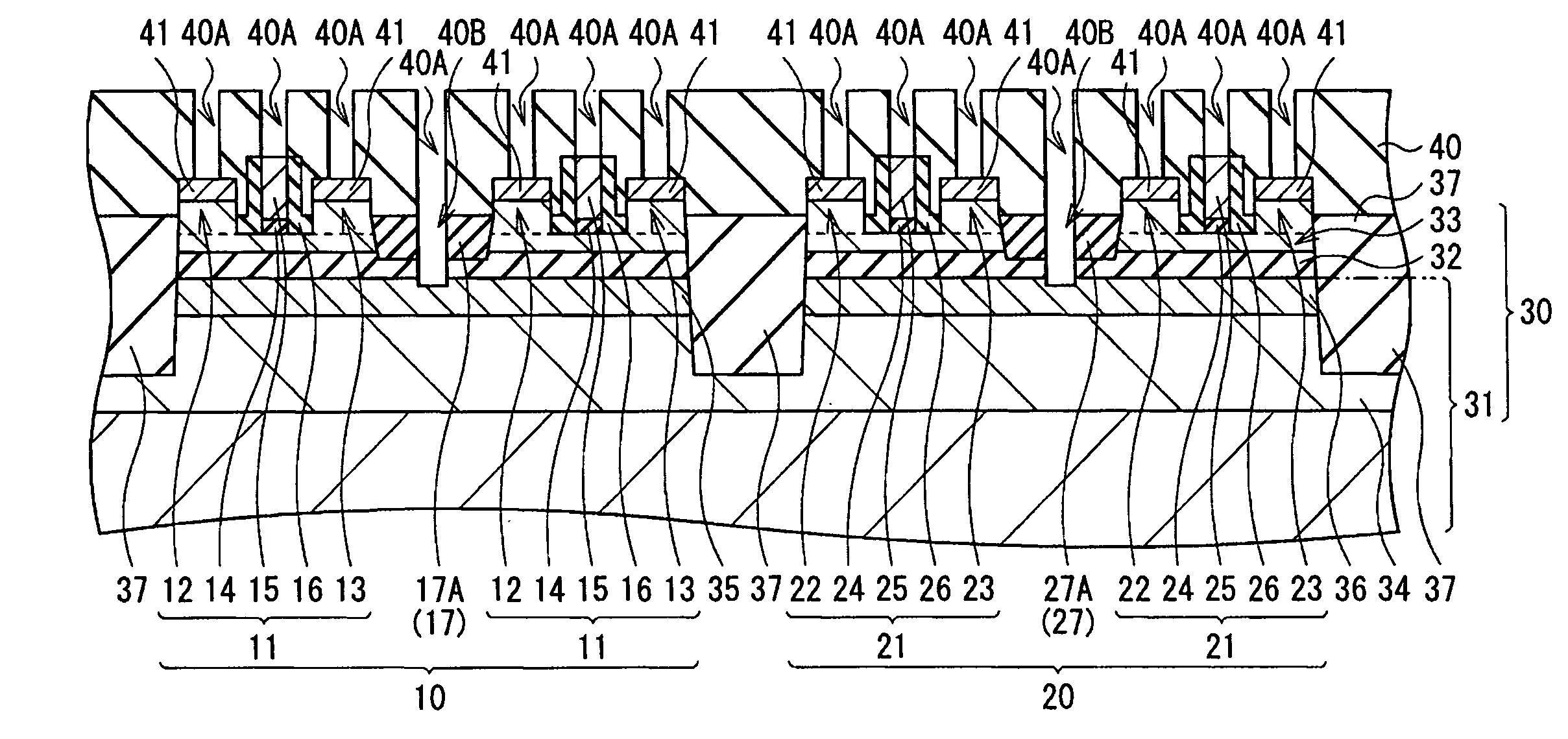
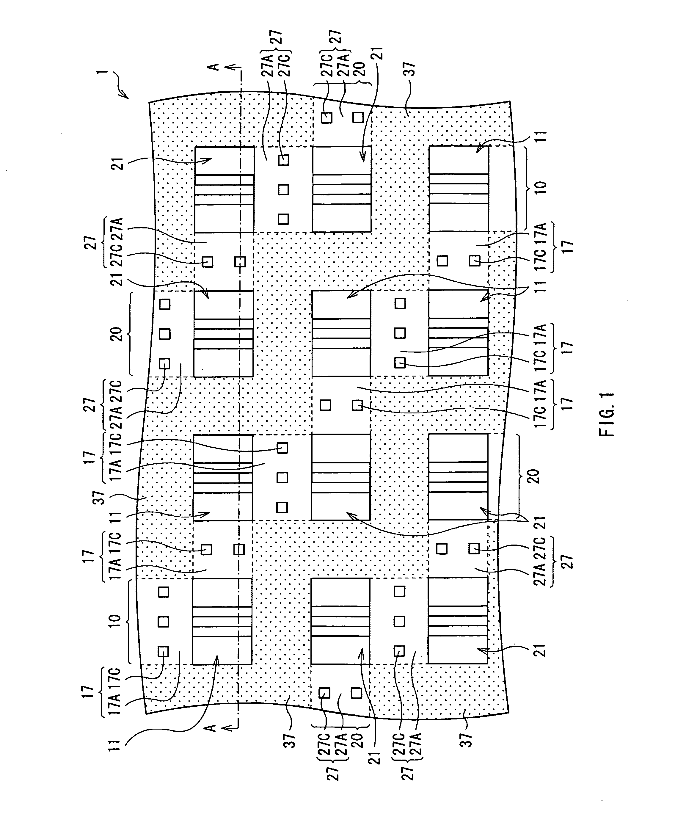
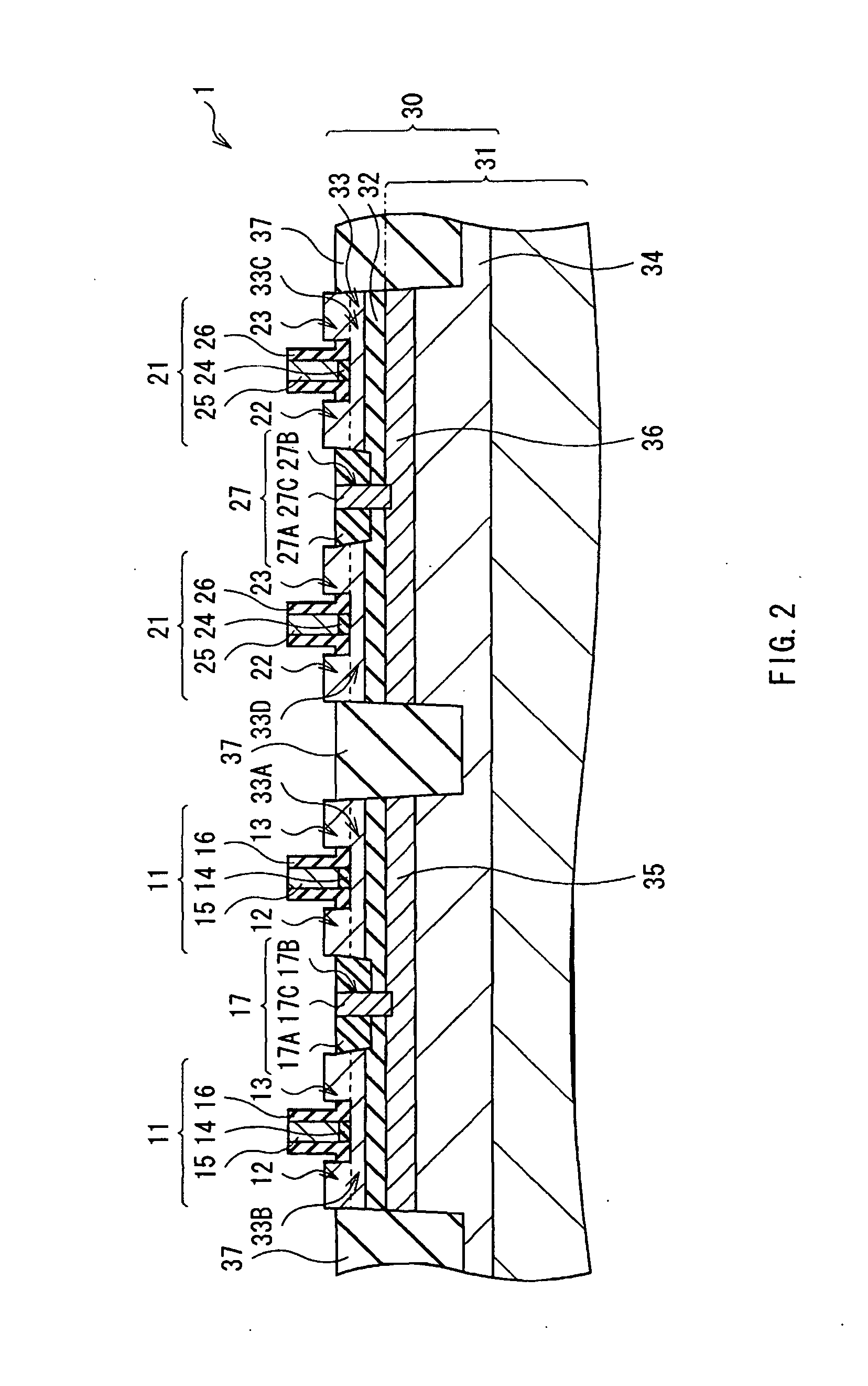
[0037]FIG. 1 illustrates an example of a top-view configuration of a semiconductor device 1 according to an embodiment of the present invention. The semiconductor device 1 is an integrated circuit in which a plurality of transistors are integrated. The semiconductor device 1 has, for example, as illustrated in FIG. 1, a first region 10 in which a plurality of p-type MOS transistors 11 are integrated and a second region 20 in which a plurality of n-type MOS transistors 21 are integrated.

Layout

[0038]The plurality of p-type MOS transistors 11 are formed in a series at a predetermined pitch in a direction in a plane. A plurality of series exist and are disposed in parallel with predetermined gaps in between. The first region 10 exists in correspondence with each series. Concretely, the first region 10 is a band-shaped region extending in the direction where the p-type MOS transistors 11 exist in series. The first regions 10 are disposed in parallel with predetermined gaps in between. In...

application example

[0081]An application example of the semiconductor device 1 of the embodiment will now be described. In the following, the case of applying the semiconductor device 1 of the embodiment to an SRAM will be described.

[0082]FIG. 13 illustrates an example of the top-view configuration of a semiconductor device 2 according to the application example. The semiconductor device 2 has an SRAM in which memory cells as storage units are disposed in a matrix and a peripheral circuit 70 of the SRAM 60. The SRAM 60 has, for example, a structure in which CMOS inverters 80 and 90 are opposed to each other as illustrated in a circuit diagram of FIG. 14.

[0083]In the CMOS inverter 80, the source or drain of a p-type MOS transistor Q1 and the source or drain of an n-type MOS transistor Q2 are connected to each other in series and the resultant is inserted in series between a power supply VDD and a ground GND. The source or drain of the p-type MOS transistor Q1 is connected to the power supply VDD side an...


PUM


Abstract

The invention provides a semiconductor device capable of suppressing a short channel effect and fluctuation in a threshold. The semiconductor device includes: a plurality of first transistors formed in a first region in a semiconductor layer in a multilayer substrate having, on a semiconductor substrate, an insulating layer and the semiconductor layer in order from the semiconductor substrate; a plurality of second transistors formed in a second region in the semiconductor layer; a first impurity layer formed in a region opposed to the first region in the semiconductor substrate; a second impurity layer formed in a region opposed to the second region in the semiconductor substrate; and a first isolation part that isolates the first and second regions from each other and electrically isolates the first and second impurity layers from each other to a degree that at least current flowing between the first and second impurity layers is interrupted.

Description

CROSS-REFERENCE TO RELATED APPLICATION[0001]The present application claims priority from Japanese Patent Application No. JP 2009-026674 filed in the Japanese Patent Office on Feb. 6, 2009, the entire content of which is incorporated herein by reference.BACKGROUND OF THE INVENTION[0002]1. Field of the Invention[0003]The present invention relates to a semiconductor device provided with two kinds of transistors of different conduction types on an insulting layer.[0004]2. Description of the Related Art[0005]With shortening of gate length, the operation speed of a MOS (Metal Oxide Semiconductor) transistor is increasing. However, power consumption also increases, and a phenomenon that total performance of an integrated circuit becomes lower than that of an existing integrated circuit is conspicuous. The phenomenon is called the short channel effect. It is extremely important to suppress the effect as much as possible in order to realize a high-performance low-power-consumption integrated...

Claims


Application Information

Patent Timeline
Patent Type & Authority Applications(United States)
IPC IPC(8): H01L27/12
CPCH01L21/823814H01L27/1203H01L21/84H01L21/823878
Inventor KIKUCHI, YOSHIAKI
Owner SONY CORP
Why Eureka
Try Eureka