Ultra thin film SOI MOSFET having recessed source/drain structure and method of fabricating the same

a technology of metal oxide semiconductor field effect transistor and ultra thin film soi mosfet, which is applied in the direction of semiconductor devices, basic electric elements, electrical equipment, etc., can solve the problems of limiting the formation of ultra shallow junctions, short channel effects, and the like, and achieve the effect of suppressing the resistance increase of the source/drain region and preventing the reduction of the drive curren

Inactive Publication Date: 2006-06-22
ELECTRONICS & TELECOMM RES INST
View PDF11 Cites 40 Cited by
  • Summary
  • Abstract
  • Description
  • Claims
  • Application Information

AI Technical Summary

Benefits of technology

[0009] The present invention provides an ultra thin film silicon on insulator (SOI) metal oxide semiconductor field effect transistor (MOSFET) having a recessed source / drain structure being capable of suppressing a resistance increase of a source / drain region, thereby preventing a reduction of a drive current due to a resistance increase of the source / drain region.

Problems solved by technology

However, as widely known, when the channel length is excessively reduced, there occurs a short channel effect.
However, with the device size being reduced down to deep-submicron of approximately 100 nm or below, typical short channel effects become more serious problems.
However, there is a limitation to form the ultra shallow junction by using a high energy ion implantation method or a high temperature diffusion process, which is now widely employed.
However, the methods both have unavoidable problems.
As a result, it occurs a serious reduction of a drive current, one of the important elements in scaling of devices.
Furthermore, even in an elevated source / drain SOI MOSFET having an elevated source / drain region formed in order to reduce a high resistance in a source / drain region when an ultra thin film SOI substrate is used, there still occurs a problem of a high resistance in a source / drain extension region for a lightly doped drain (LDD) structure.
The problem becomes more serious with an integration of a device being increased.

Method used


Image

  • Ultra thin film SOI MOSFET having recessed source/drain structure and method of fabricating the same
  • Ultra thin film SOI MOSFET having recessed source/drain structure and method of fabricating the same
  • Ultra thin film SOI MOSFET having recessed source/drain structure and method of fabricating the same

Examples


Embodiment Construction

[0024] The present invention will now be described more fully hereinafter with reference to the accompanying drawings, in which preferred embodiments of the invention are shown. This invention may, however, be embodied in many different forms and should not be construed as being limited to the embodiments set forth herein. Rather, these embodiments are provided so that this disclosure will be thorough and complete, and will fully convey the scope of the invention to those skilled in the art. Like numbers refer to like elements throughout the specification.

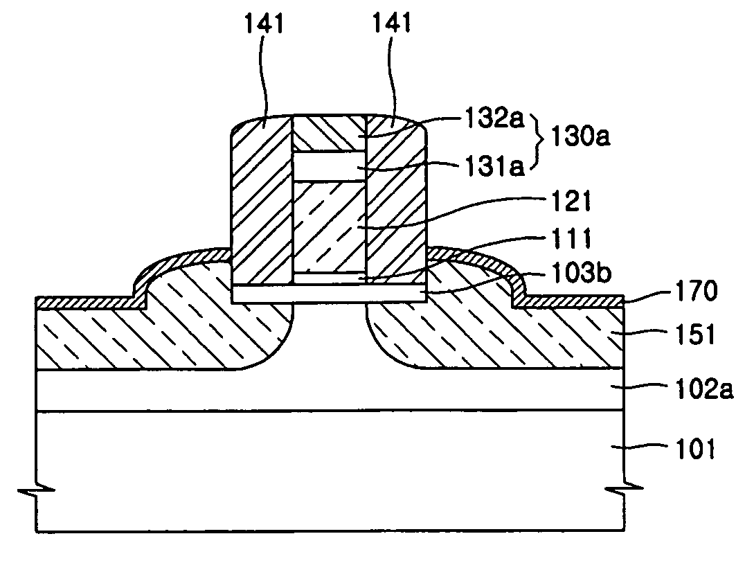
[0025]FIG. 13 is a sectional view illustrating a thin film silicon on insulator (SOI) metal oxide semiconductor field effect transistor (MOSFET) according to the present invention.

[0026] Referring to FIG. 13, in the ultra thin film SOI MOSFET of the present invention, a recessed buried oxide layer 102a is disposed on a single crystalline substrate 101. The recessed buried oxide layer 102a is structured being recessed at its rest ...


PUM


Abstract

There are provided an ultra thin film silicon on insulator (SOI) metal oxide semiconductor field effect transistor (MOSFET) having a recessed source/drain structure, and a method of fabricating the same. The ultra thin film SOI MOS transistor includes a semiconductor substrate; a buried insulating layer disposed on the semiconductor substrate, and formed recessed except for a center portion thereof; an ultra thin film single crystalline silicon layer pattern disposed on the recessed buried insulating layer; a gate stack disposed on the ultra thin film single crystalline silicon layer pattern, and including a gate insulating layer pattern and a gate conductive layer pattern, which are sequentially stacked; a gate spacer layer disposed on sidewalls of the gate stack; and a recessed source/drain region disposed on the recessed buried insulating layer, and formed to overlap a bottom surface portion of the ultra thin film single crystalline silicon layer pattern, which does not overlap the center portion of the recessed buried insulating layer.

Description

CROSS-REFERENCE TO RELATED PATENT APPLICATION [0001] This application claims the benefit of Korean Patent Application No. 10-2004-0108155, filed on Dec. 17, 2004, in the Korean Intellectual Property Office, the disclosure of which is incorporated herein in its entirety by reference. BACKGROUND OF THE INVENTION [0002] 1. Field of the Invention [0003] The present invention relates to a method of fabricating a semiconductor device, and an ultra thin film silicon on insulator (SOI) metal oxide semiconductor field effect transistor (MOSFET) having a recessed source / drain structure, and a method of fabricating the same. [0004] 2. Description of the Related Art [0005] Recently, with the increase of demand for a low power consumption, a high integration, an ultra high speed device characteristics of semiconductor devices, and the like, it is also required that a size of a MOS transistor employed in various semiconductor devices be reduced. In specific, it is required that a channel length o...

Claims


Application Information

Patent Timeline
Patent Type & Authority Applications(United States)
IPC IPC(8): H01L27/12
CPCH01L29/66636H01L29/66772H01L29/78618H01L29/7824
Inventor AHN, CHANG GEUNCHO, WONJUIM, KIJUYANG, JONG HEONBAEK, IN BOKLEE, SEONG JAEBAEK, SUNG KWEON
Owner ELECTRONICS & TELECOMM RES INST
Why Eureka
Try Eureka