Flash memory cell, flash memory device and manufacturing method thereof

a flash memory and flash memory technology, applied in semiconductor devices, solid-state devices, instruments, etc., can solve the problems of narrow process margins, pattern non-uniformity, and memory cell size reduction, and achieve high density of memory cells, reduce parasitic coupling noise of adjacent floating gates, and reduce short channel effects.

Inactive Publication Date: 2006-08-08
POLARIS INNOVATIONS LTD
View PDF13 Cites 37 Cited by
  • Summary
  • Abstract
  • Description
  • Claims
  • Application Information

AI Technical Summary

Benefits of technology

[0012]In view of the above, it is a first object of the invention to provide non-volatile flash memory cells allowing a very high dense integration of memory cells, which are qualified to produce mass storage flash memories of 4 GBit and higher, which are especially capable of reducing parasitic coupling noise of adjacent floating gates and of reducing short channel effects, and which are capable of enhancing signal-to-noise ratio of the sense current.
[0026]Recently, as for instance is disclosed in the above-referenced document of Ichige et al., self-aligned STI (shallow trench isolation) technology has been reported to be effectively used in reduced memory cell size production in order to realize highly integrated flash memory devices. Moreover, STI-technology may provide a reduced number of fabrication steps during manufacture of the integrated circuit device, thus requiring low fabrication costs and offering high reliability.

Problems solved by technology

Therefore, one of the most important issues for low-cost and high-density mass storage flash memories is a reduction of the memory cell size.
However, in down-scaling flash memories a lot of problems arise, such as pattern nonuniformity and narrow process margins.
Also, parasitic coupling noise increases, which may especially cause severe problems relating to adjacent floating gates in NAND-type memory cell arrays.
Otherwise, especially in NAND-type memory cell arrays having a plurality of memory cells connected in a serial array, reducing of channel width may lead to a decrease of the sense current through the memory cells, for which reason, signal-to-noise-ratio is deteriorated.
While such FinFET-memory cells may actually succeed in enhancing signal-to-noise ratio, they, however, are usually not suitable for application in a high-density mass storage array due to a too large-sized floating gate.
Other solutions especially for overcoming the above-identified problem of reducing signal-to-noise ratio (see for example U.S. patent application 2003 / 0178670 to Fried et al.) comprise floating gates to be splitted in two parts by specific manufacturing methods, which, however, because of unavoidably occurring process variations may lead to a unsymmetric programming effect and erasing effect, respectively.
Furthermore, convenient manufacturing methods as disclosed in the above-cited documents may not lead to a high-dense architecture of mass storage flash memory devices.

Method used


Image

  • Flash memory cell, flash memory device and manufacturing method thereof
  • Flash memory cell, flash memory device and manufacturing method thereof
  • Flash memory cell, flash memory device and manufacturing method thereof

Examples


Embodiment Construction

[0043]Embodiments of the present invention will be described in detail below with reference to the accompanying drawings, where like designations denote like elements.

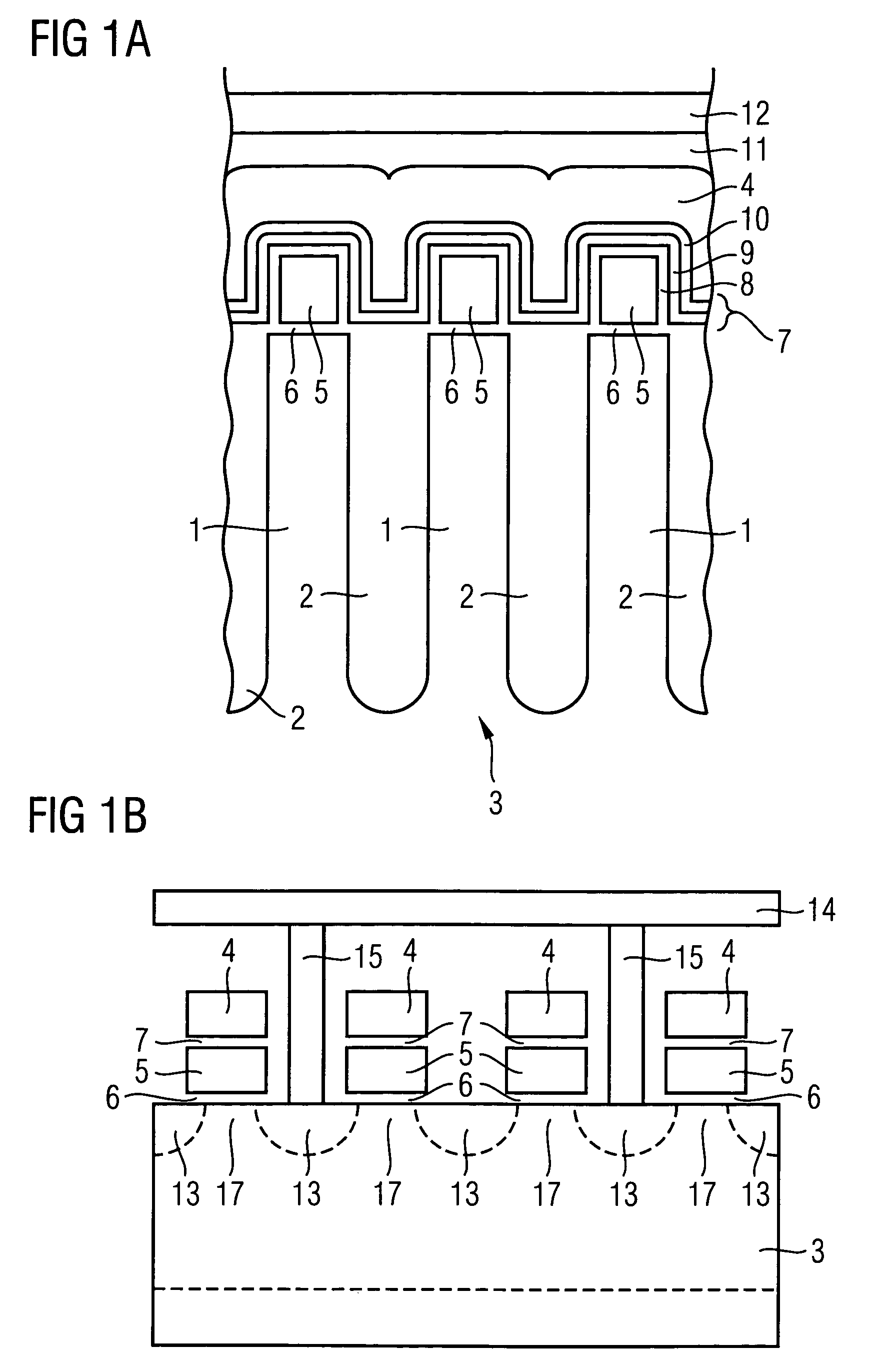
[0044]FIGS. 1A and 1B are schematic cross-sectional views showing prior art high-density flash memory cells being of NAND-type and NOR-type structure, respectively. FIGS. 5A and 5B are schematic top plan views showing an array of flash memory cells having NAND-type structure and NOR-type structure, respectively. These figures have already been described in the introductory portion, for which reason an explanation may be omitted to avoid unnecessary repetitions.

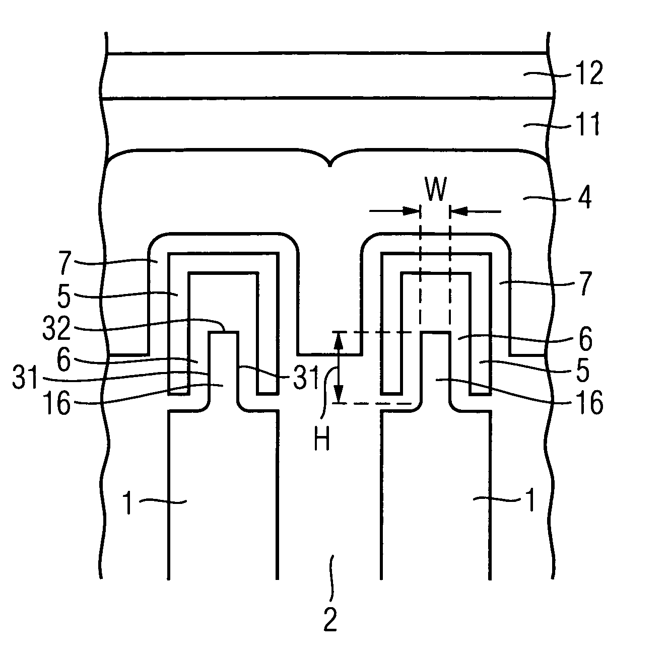
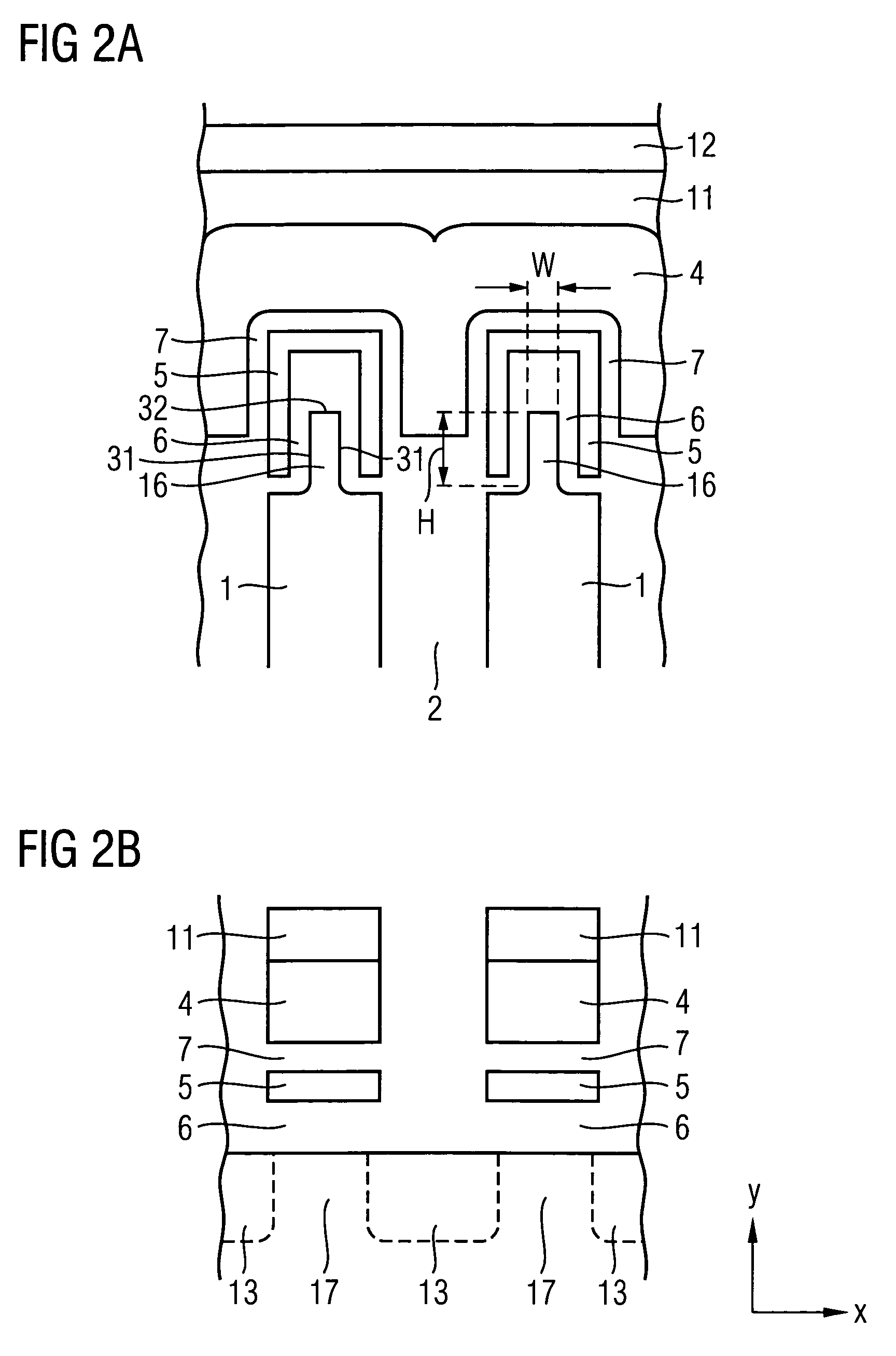
[0045]Referring now to FIGS. 2A and 2B, schematic cross-sectional views showing a preferred embodiment of high-density flash memory cells being of NAND-type structure according to the invention are illustrated. FIG. 2A shows a cross-sectional view along the word line, which is identified by control gate 4, whereas FIG. 2B shows a cross-sectional view along the bi...


PUM


Abstract

The present invention relates to a flash memory cell comprising a silicon substrate having an active region comprising a channel region and source- / drain-regions, the active region comprising a projecting portion, which projecting portion at least comprising said channel region; a tunneling dielectric layer formed on the surface of said active region; a floating gate formed on the surface of said tunneling dielectric layer for storing electric charges; an inter-gates coupling dielectric layer formed on the surface of said floating gate, and a control gate formed on the surface of said inter-gates coupling dielectric layer, wherein said floating gate is formed to have a groove-like shape for at least partly encompassing said projecting portion of said active region. This invention further relates to a flash memory device comprising such flash memory cells, as well as a manufacturing method thereof.

Description

TECHNICAL FIELD[0001]This invention is in the field of non-volatile semiconductor memory devices and more particularly relates to a flash memory cell, a flash memory device comprising an array of such flash memory cells, such as a NOR-type flash memory device or a NAND-type flash memory device, and a manufacturing method thereof.BACKGROUND ART[0002]A non-volatile flash memory device is known to store charges in a floating gate by means of either Fowler-Nordheim tunneling or hot-electron injection through a thin tunneling-oxide layer from a semiconductor substrate for programming operation and to remove or erase charges stored in a floating gate by means of Fowler-Nordheim tunneling through a thin tunneling-oxide layer to a semiconductor substrate or to a control gate for erasing operation. Based on the specific cell structure chosen, flash memory cells may be made up of a stack-gate structure.[0003]A typical stack-gate structure of prior art flash memory cells is shown in FIG. 1A an...

Claims


Application Information

Patent Timeline
Patent Type & Authority Patents(United States)
IPC IPC(8): H01L29/76H01L29/788G11C16/02H01L21/336H01L21/8247H01L27/115H01L29/786
CPCH01L27/115H01L27/11521H01L29/78645H01L29/7851H01L29/66818H10B69/00H10B41/30
Inventor WILLER, JOSEFLAU, FRANK
Owner POLARIS INNOVATIONS LTD
Why Eureka
Try Eureka