Graphene-based waveguide integrated multimode electro-optic modulator and manufacturing method thereof

An electro-optical modulator and waveguide integration technology, applied in the field of integrated optics, can solve the problems of increasing equipment cost and volume, affecting the application of mode division multiplexing technology, and being unfavorable for high integration and temperature control of on-chip devices, so as to facilitate high-density integration. , the effect of large carrier mobility, low energy consumption and heat

Active Publication Date: 2019-09-10
TIANJIN UNIV
View PDF13 Cites 5 Cited by
  • Summary
  • Abstract
  • Description
  • Claims
  • Application Information

AI Technical Summary

Problems solved by technology

It is impossible to modulate different modes in the same device at the same time, which increases the cost and volume of the device to a certain extent, which is not conducive to the high integration and temperature control of on-chip devices
[0005] In summary, although the mode division multiplexing technology has been developed rapidly in recent years, each mode requires separate modulation, which affects the application of the mode division multiplexing technology in integrated optics.

Method used


Image

  • Graphene-based waveguide integrated multimode electro-optic modulator and manufacturing method thereof
  • Graphene-based waveguide integrated multimode electro-optic modulator and manufacturing method thereof
  • Graphene-based waveguide integrated multimode electro-optic modulator and manufacturing method thereof

Examples


Embodiment 1

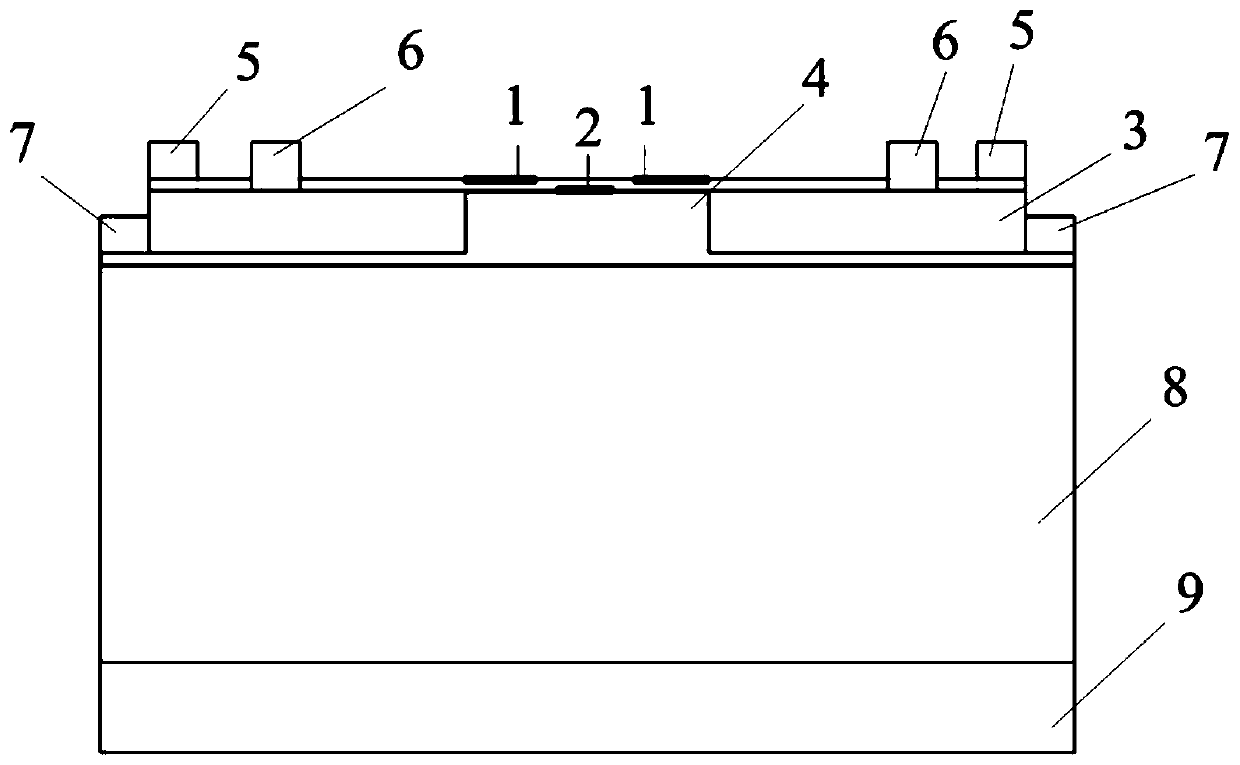
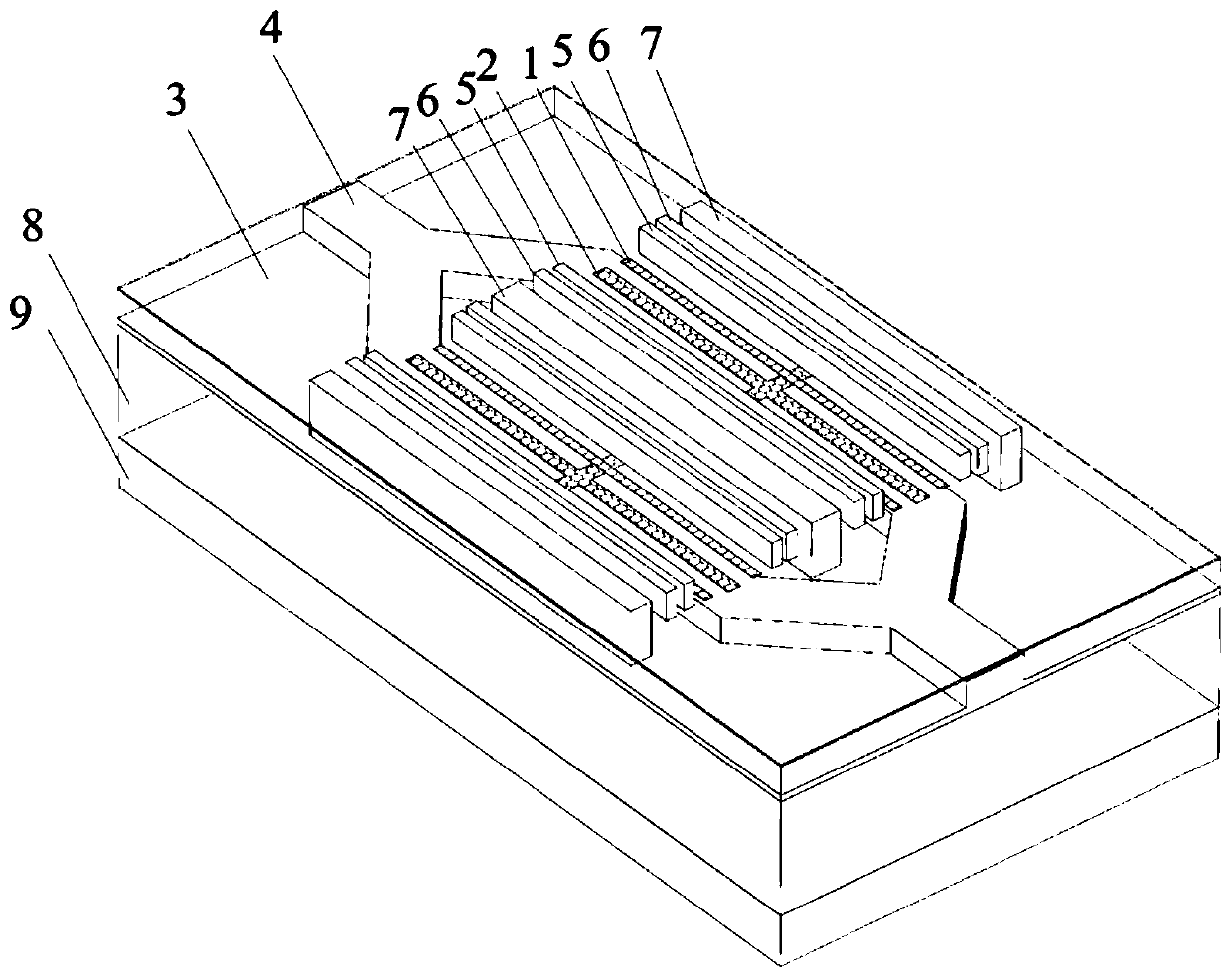
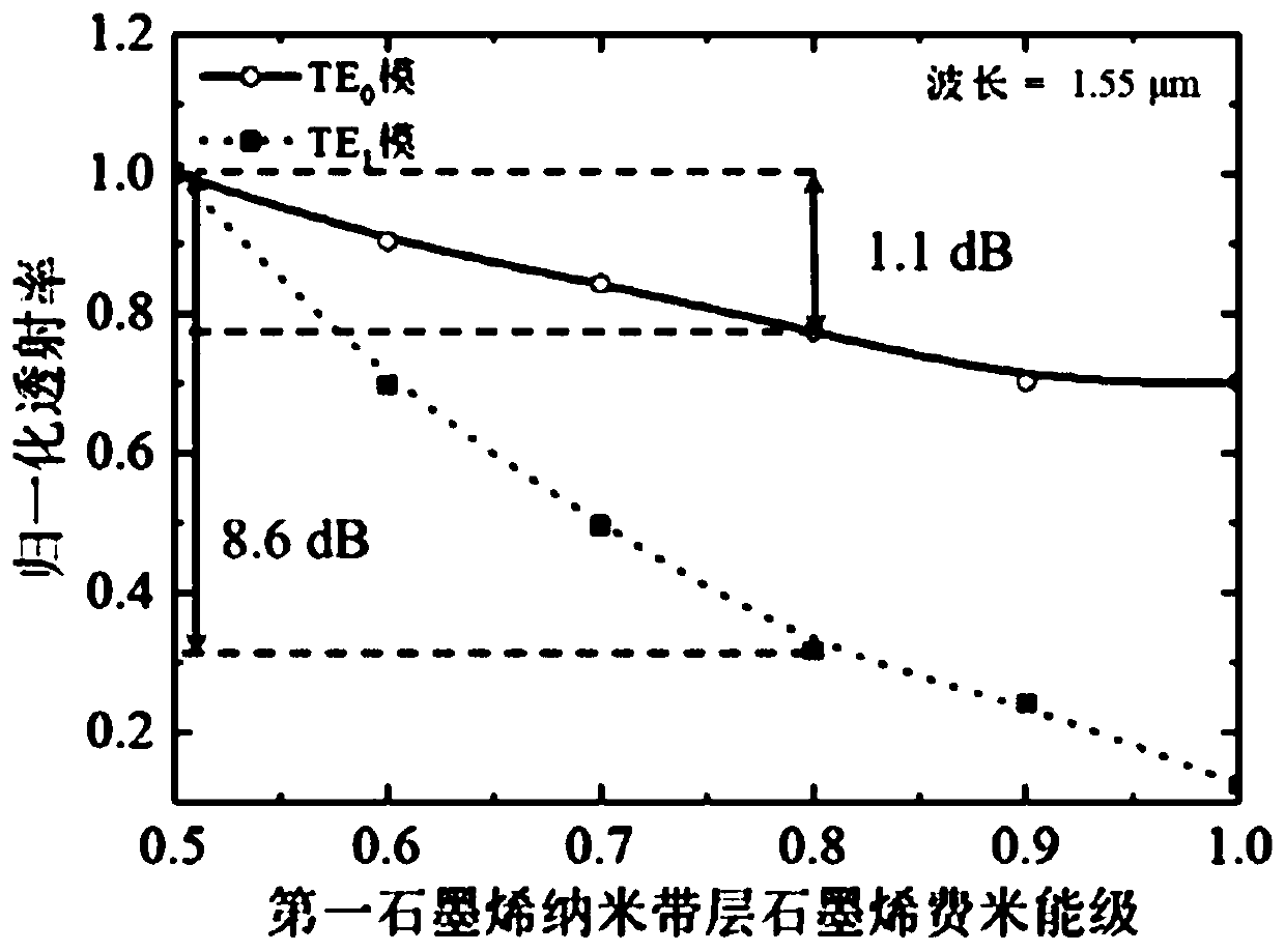
[0030] Such as figure 2 The shown graphene-based waveguide integrated multimode electro-optical modulator: the graphene width of the first graphene nanoribbon layer 1 is 300nm, the graphene width of the second graphene nanoribbon layer 2 is 350nm, and the waveguide width is 1μm , The height of the multimode ridge waveguide 4 is 250nm, and the multimode electro-optic modulator integrated with the graphene-based waveguide is designed as a Mach-Zehnder modulator with two arms length of 350nm. In the initial state, the Fermi levels of the first graphene nanoribbon layer and the second graphene nanoribbon layer of both arms are adjusted to 0.4 eV. Such as Figure 3-1 with Figure 3-2 As shown, the graphene and TE are changed by changing the Fermi level of the first graphene nanoribbon layer to 0.8eV 0 With TE 1 Mode interaction, due to the first graphene nanoribbon layer and TE 1 Strong mode effect, TE 0 Mode effect is weak, TE 1 The optical phase shift of the mode is large, TE 0 Th...

Embodiment 2

[0033] Such as Figure 4 The shown graphene-based waveguide integrated multimode electro-optical modulator: the graphene width of the first graphene nanoribbon layer 1 is 300nm, the graphene width of the second graphene nanoribbon layer 2 is 350nm, and the waveguide width is 1μm , The height of the multimode ridge waveguide 4 is 250nm, and the multimode modulator integrated with the graphene-based waveguide is designed as a micro-race resonant cavity modulator, which is a kind of micro-ring resonator. The length of the straight waveguide in the channel resonator is 228.5 μm, the radius of the semicircle in the micro-race cavity is 30 μm, and the distance between the straight waveguide of the micro-race cavity and the coupled straight waveguide 10 is 344 nm. Choose 1.55237μm as the detection wavelength. Such as Figure 5-1 to Figure 5-4 As shown, in the initial state, the Fermi level of the first graphene nanoribbon layer is adjusted to 0.45 eV, and the Fermi level of the secon...


PUM


Abstract

The invention discloses a graphene-based waveguide integrated multimode electro-optic modulator and a manufacturing method thereof. The modulator comprises a first graphene nanoribbon layer, a secondgraphene nanoribbon layer, an insulator cladding, a multimode ridge waveguide, a first electrode pair, a second electrode pair, a third electrode pair, an insulating layer and a substrate layer, wherein the multimode ridge waveguide supports two transverse electric modes (TE), that is, a TE0 mode and a TE1 mode are simultaneously transmitted; the first graphene nanoribbon layer and the second graphene nanoribbon layer are integrated above the multimode ridge waveguide; the insulator cladding is used to achieve electrical isolation of the multimode ridge waveguide from the first graphene nanoribbon layer and the second graphene nanoribbon layer; the first electrode pair is connected to the first graphene nanoribbon layer, the second electrode pair is connected to the second graphene nanoribbon layer, and the third electrode pair is coupled to the multimode ridge waveguide for providing a back gate voltage to the graphene.

Description

Technical field [0001] The invention relates to the technical field of integrated optics, in particular to a graphene-based waveguide integrated multi-mode electro-optic modulator and a manufacturing method. Background technique [0002] In the past few years, graphene-silicon-based hybrid integrated optical circuits have attracted great attention. Because graphene has ultra-high carrier mobility and adjustable Fermi level, the absorption of light by graphene can be quickly adjusted through the band filling effect, and can be used to develop high-speed optoelectronic devices. In addition, by combining graphene with a silicon waveguide, light propagating in the silicon waveguide can interact with the surface-integrated graphene through the evanescent field. This structure makes full use of the unique physical properties of monoatomic layer graphene, and at the same time is not affected by the weak light-matter interaction in the atomic layer thick graphene. So far, based on the ...

Claims


Application Information

Patent Timeline
Patent Type & Authority Applications(China)
IPC IPC(8): G02B6/12G02B6/13
CPCG02B6/12G02B6/13G02B2006/12035G02B2006/12085G02B2006/1209G02B2006/12142G02B2006/12166
Inventor 程振洲邢正锟韩迎东胡浩丰刘铁根
Owner TIANJIN UNIV
Why Eureka
Try Eureka