Semiconductor optical modulation device

a technology of optical modulation and semiconductor, applied in the direction of optics, semiconductor lasers, instruments, etc., can solve the problems of difficult to achieve long distance transmission for a distance of 40 km or more by uncooled operation, and the method is not suitable for the operation in the 1550 nm band of signal light wavelength

Active Publication Date: 2007-10-11
LUMENTUM JAPAN INC
View PDF5 Cites 12 Cited by
  • Summary
  • Abstract
  • Description
  • Claims
  • Application Information

AI Technical Summary

Benefits of technology

[0023] The present invention provides a light emission device using an EA modulator having optimal detuning in the 1550 nm band and a quantum well structure suitable for a long distance optical communication for a distance of 40 km or more, thereby providing an inexpensive light source.

Problems solved by technology

However, using the methods described above means to increase chirping.
The methods are not suitable for the operation in the 1550 nm band of the signal light wavelength.
The long distance transmission for a distance of 40 km or more by the uncooled operation is difficult to be attained.

Method used


Image

  • Semiconductor optical modulation device
  • Semiconductor optical modulation device
  • Semiconductor optical modulation device

Examples


embodiment 1

RWG-EA / DFB (DBR)

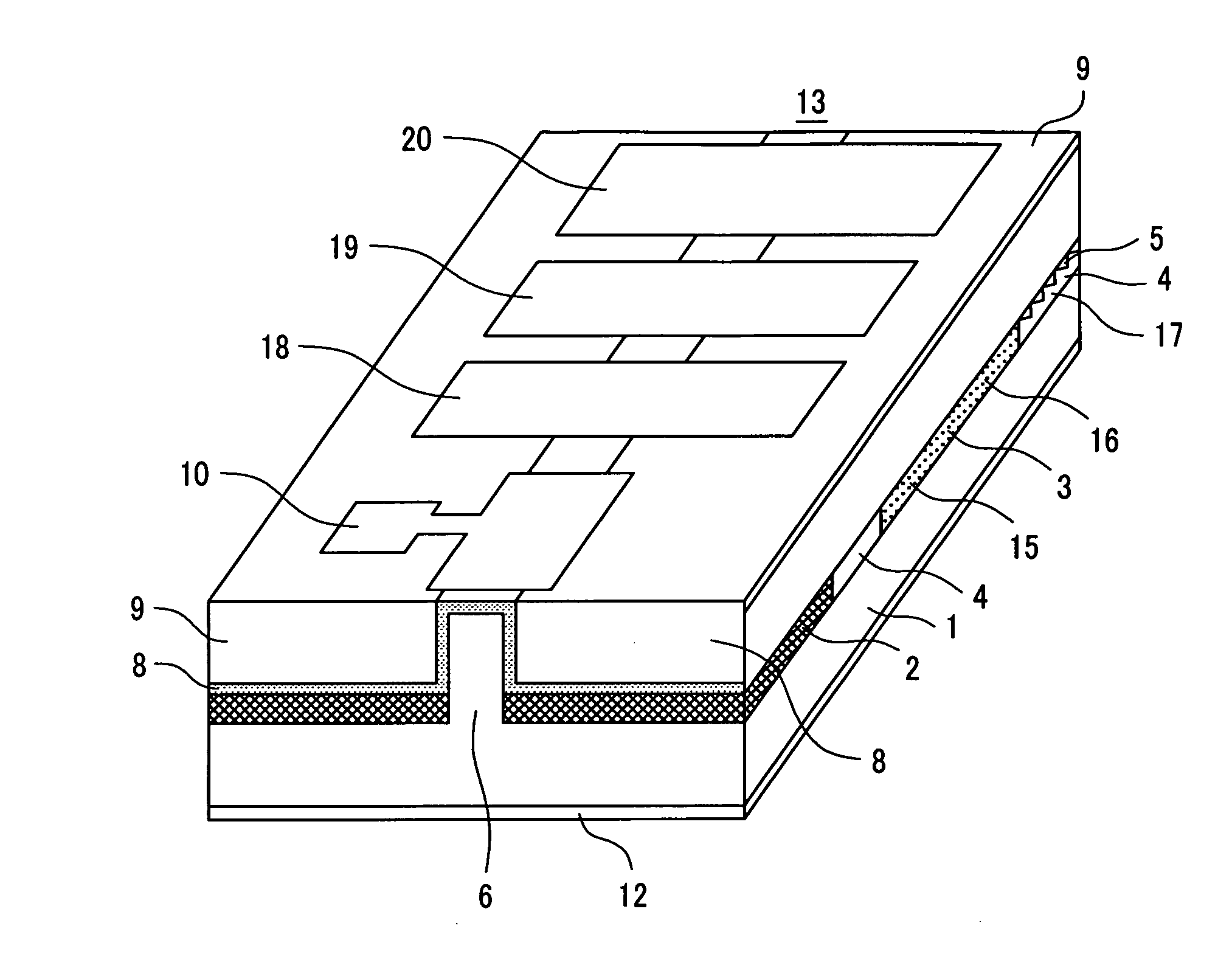
[0054] A process for manufacturing a semiconductor optical integrated device according to Embodiment 1 of the present invention is described with reference to FIG. 5 and FIG. 6. The drawings are only for the purpose of explaining the embodiment. The size and scale of the drawings showing the embodiment are not necessarily identical.

[0055] At first, a quantum well structure 2 made of an InGaAlAs system is formed on an n-InP substrate 1 as an electro-absorption optical modulator using an MOCVD method (FIG. 5A). In this case, a light emission wavelength of the quantum well structure at a temperature of 25° C. is about 1470 nm. For example, a desired light emission wavelength can be obtained by laminating a quantum well layer with a thickness of 6 nm and with a compositional ratio of In, Ga, and Al at 0.54:0.38:0.08, and a barrier layer with a thickness of 10 nm and with a compositional ratio of In, Ga, and Al at 0.52:0.33:0.15. Further, an optical confinement structur...

embodiment 2

BH-EA / DFB (DBR)

[0070]FIG. 7A is a perspective view illustrating a construction according to another embodiment of a semiconductor optical integrated device applied with the present invention. FIG. 7B is a perspective view illustrating a cross section cut along a central line. However, the drawing is only for explaining this embodiment and the size and scale of the drawing showing this embodiment are not necessarily identical.

[0071] At first, a quantum well structure 2 made of an InGaAlAs system is formed on an n-InP substrate 1 as an electro-absorption optical modulator using an MOCVD method. In this case, a light emission wavelength of the quantum well structure 2 at a temperature of 25° C. is about 1470 nm. For example, a desired light emission wavelength can be obtained by laminating a quantum well layer with a thickness of 6 nm and with a compositional ratio of In, Ga, and Al at 0.54:0.38:0.08, and a barrier layer with a thickness of 10 nm and with a compositional ratio of In,...

embodiment 3

RWG-EA / Variable Wavelength LD

[0085]FIG. 8A is a perspective view showing the constitution according to another embodiment of a semiconductor optical integrated device formed as a variable wavelength LD applied to the present invention. FIG. 8B is a perspective view illustrating a cross section cut along a central line. Figures for the processes shown in FIGS. 5 and 6 in Embodiment 1 are not illustrated. However, the drawing is only for the explanation of this embodiment and the size and scale of the drawing showing this embodiment are not necessarily identical.

[0086] A quantum well structure 2 made of an InGaAlAs system is formed on an n-InP substrate 1 as an electro-absorption optical modulator using an MOCVD method. In this case, a light emission wavelength of the quantum well structure at a temperature of 25° C. is about 1470 nm. For example, a desired light emission wavelength can be obtained by forming a quantum well layer with a thickness of 6 nm and with a compositional rat...


PUM


Abstract

In a conventional EA/DFB laser, since the temperature dependence of the operation wavelength of the EA portion is substantially different from that of the DFB portion, the temperature range over which a stable operation is possible is small. In the case of using the EA/DFB laser as a light emission device, an uncooled operation is not possible. An EA/DFB laser which does not require a temperature control mechanism is proposed. A quantum well structure in which a well layer made of any one of InGaAlAs, InGaAsP, and InGaAs, and a barrier layer made of either one of InGaAlAs or InAlAs is used for an optical absorption layer of an EA modulator. By properly determining detuning at a temperature of 25° C. and a composition wavelength of the barrier layer in the quantum well structure used for the optical absorption layer, it can be realized to suppress the insertion loss, maintain the extinction ratio, and reduce chirping simultaneously over a wide temperature range from −5° C. to 80° C.

Description

CLAIM OF PRIORITY [0001] The present invention application claims priority from Japanese application JP 2006-105932 filed on Apr. 7, 2006 the content of which is hereby incorporated by reference into this application. FIELD OF THE INVENTION [0002] The present invention relates to a semiconductor optical modulation device and an integrated semiconductor light emission device integrating the same. BACKGROUND OF THE INVENTION [0003] With the proliferation of broad band networks, the trend of increasing the communication speed to 10 Gbit / s or higher has been accelerated in metropolitan optical communication networks connecting cities and relay stations. In the metropolitan optical communication networks, a fiber transmission distance of 40 to 80 km has been demanded for long distance transmission. In an optical communication system for the metropolitan optical communication network, it is an important subject to reduce the size and the power consumption of the optical transmitter / receiv...

Claims


Application Information

Patent Timeline
Patent Type & Authority Applications(United States)
IPC IPC(8): H01L29/06
CPCB82Y20/00G02F2001/0157H01S5/0265G02F1/01708G02F1/0157
Inventor MAKINO, SHIGEKI
Owner LUMENTUM JAPAN INC
Why Eureka
Try Eureka