Digital resistive type touch panel and fabrication method thereof

a technology of resistive type and touch panel, which is applied in the direction of identification means, instruments, computing, etc., can solve the problems of inability of the general capacitive type touch panel to detect the location of the touched point correctly, suffer from inaccuracy and low resolution, and the input device of the keyboard and the mouse has a limit in coping with the demand as an interfa

Active Publication Date: 2008-04-08
LG DISPLAY CO LTD
View PDF10 Cites 112 Cited by
  • Summary
  • Abstract
  • Description
  • Claims
  • Application Information

AI Technical Summary

Benefits of technology

[0015]An advantage of the present invention is to provide a touch panel which can use various types of input means, irrespective of whether the input is conductive, so that, in addition to conductive means, a gloved hand or a non-conductive stylus pen can be used as an input means.
[0016]Additional advantages, objects, and features of the invention will be set forth in part in the description which follows and in part will become apparent to those having ordinary skill in the art upon examination of the following or may be learned from practice of the invention. The objectives and other advantages of the invention may be realized and attained by the structure particularly pointed out in the written description and claims hereof as well as the appended drawings.
[0017]To achieve these objects and other advantages and in accordance with the purpose of the invention, as embodied and broadly described herein, a touch panel may, for example, include a supporting substrate; a first transparent conductive layer having first a electrode for applying a voltage to the supporting substrate; a second transparent conductive layer having a second electrode and facing the first transparent conductive layer; an adhesive for attaching the first and second transparent conductive layers to each other; and a passivation film on an outer surface of the second transparent conductive layer.
[0018]In another aspect of the present invention, a method of fabricating a touch panel integrated with a display device may, for example, include providing a supporting substrate; forming a first transparent conductive layer having a first electrode for applying a voltage to the supporting substrate; forming a second transparent conductive layer having a second electrode and facing the first transparent conductive layer; attaching the first and second transparent conductive layers to each other using an adhesive; and forming a passivation film on an outer surface of the second transparent conductive layer.
[0019]In another aspect of the present invention, a liquid crystal display device integrated with a touch panel may, for example, include the touch panel having a supporting substrate having first and second surfaces, a first transparent conductive layer on the first surface of the supporting substrate, the first transparent conductive layer having a first electrode for applying a voltage to the supporting substrate, a second transparent conductive layer having a second electrode and facing the first transparent conductive layer, an adhesive between the first and second transparent conductive layers, and a passivation film on an outer surface of the second transparent conductive layer; and the liquid crystal display device on the second surface of the supporting substrate of the touch panel, the liquid crystal display device having a first substrate having a plurality of thin film transistors, a second substrate having a color filter and facing the first substrate, and a liquid crystal layer between the first and second substrates.
[0020]In yet another aspect of the present invention, a method for fabricating a liquid crystal display device integrated with a touch panel may, for example, include providing a supporting substrate having first and second surfaces; forming a first transparent conductive layer on the first surface of the supporting substrate, the first transparent conductive layer having a first electrode for applying a voltage to the supporting substrate; forming a second transparent conductive layer having a second electrode and facing the first transparent conductive layer; attaching the first and second transparent conductive layers to each other using an adhesive; forming a passivation film on an outer surface of the second transparent conductive layer; and forming the liquid crystal display device on the second surface of the supporting substrate of the touch panel, the method for fabricating the liquid crystal display device including preparing a first substrate having a plurality of thin film transistors, preparing a second substrate having a color filter and facing the first substrate, and providing a liquid crystal layer between the first and second substrates.

Problems solved by technology

As personal information devices are in demand in various fields, the input devices of the keyboard and the mouse have a limit in coping with the demand as an interface.
Accordingly, when a gloved hand is used or when a conductive stylus pen is unavailable, it is hard for the general capacitive type touch panel to detect the location of a touched point correctly.
However, unlike the capacitive type touch panel, since the resistive type touch panel detects the location of a touched point according to the resistance of the transparent conductive layer, it suffers from inaccuracy and low resolution, compared with the capacitive type touch panel.

Method used


Image

  • Digital resistive type touch panel and fabrication method thereof
  • Digital resistive type touch panel and fabrication method thereof
  • Digital resistive type touch panel and fabrication method thereof

Examples


Embodiment Construction

[0032]Reference will now be made in detail to an embodiment of the present invention, example of which is illustrated in the accompanying drawings. Wherever possible, the same reference numbers will be used throughout the drawings to refer to the same or like parts.

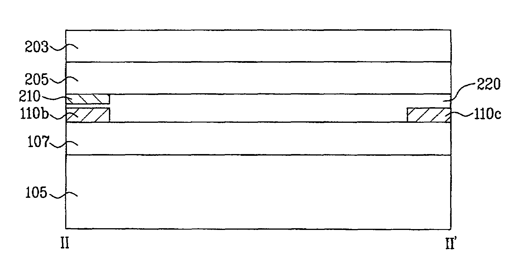
[0033]FIG. 5A and FIG. 5B are plan views illustrating lower and upper films of a touch panel according to the present invention, respectively. FIG. 6 is a plan view illustrating a bonding state between the lower and upper films of FIG. 5A and FIG. 5B. FIG. 7 is a cross-sectional view taken along line II-II′ of FIG. 5A, FIG. 5B and FIG. 6. FIG. 8 is a cross-sectional view taken along line III-III′ of FIG. 6.

[0034]In the touch panel according to the present invention, a glass substrate 105 is provided as a supporting substrate. Then, as shown in FIG. 5A, after forming a first transparent conductive layer 107, metal electrodes 110a, 110b, 110c and 110d are respectively formed at four corners of the first transparent conducti...


PUM


Abstract

A display device integrated with a touch panel is disclosed, which can use various types of input devices. Thus, in addition to conductive devices, a gloved hand or a non-conductive stylus pen can be used as an input. The touch panel includes a supporting substrate; a first transparent conductive layer having a first electrode for applying a voltage to the supporting substrate; a second transparent conductive layer having a second electrode and facing the first transparent conductive layer; an adhesive for attaching the first and second transparent conductive layers to each other; and a passivation film on an outer surface of the second transparent conductive layer.

Description

[0001]This application claims the benefit of the Korean Application No. P2002-83300 filed on Dec. 24, 2002, which is hereby incorporated by reference for all purposes as if fully set forth herein.BACKGROUND OF THE INVENTION[0002]1. Field of the Invention[0003]The present invention relates to a display device integrated with a touch panel, and more particularly, to a liquid crystal display device integrated with a touch panel capable of using various input devices, including conductive and nonconductive types, and its fabrication method.[0004]2. Discussion of the Related Art[0005]For personal information devices, such as personal computers and mobile transmission devices, a variety of input devices, such as a keyboard, a mouse and a digitizer, have been generally used for text and graphic processes. As personal information devices are in demand in various fields, the input devices of the keyboard and the mouse have a limit in coping with the demand as an interface. Thus, it is benefi...

Claims


Application Information

Patent Timeline
Patent Type & Authority Patents(United States)
IPC IPC(8): G09G5/00G06F3/03G06F3/14G09F9/35
CPCG06F3/044G06F3/045G06F2203/04103G06F3/0444G06F3/03G06F3/0445
Inventor HONG, HEE JUNGPARK, HEE JEONG
Owner LG DISPLAY CO LTD
Why Eureka
Try Eureka