Field emission display having grid plate with multi-layered structure

a multi-layered structure and field emission technology, applied in the field of field emission display, can solve the problem of difficult manufacturing of feed, and achieve the effect of reducing the width of the grid plate, preventing the illumination of unintended pixels, and reducing the size of the opening of the grid pla

Inactive Publication Date: 2008-04-29
SAMSUNG SDI CO LTD
View PDF18 Cites 3 Cited by
  • Summary
  • Abstract
  • Description
  • Claims
  • Application Information

AI Technical Summary

Benefits of technology

[0014]In one exemplary embodiment of the present invention, there is provided a field emission display that minimizes a size of openings of a grid plate while avoiding the problems associated with a decreased width of the grid plate, thereby preventing the illumination of unintended pixels by the spreading of electron beams. Also, the field emission display mounts the grid plate without the use of lower spacers to avoid the difficulties involved in arranging the lower spacers during manufacture.

Problems solved by technology

However, this approach can cause the manufacture of the FED to be difficult as a result of the complications involved in having to arrange a larger number of lower spacers 21.

Method used


Image

  • Field emission display having grid plate with multi-layered structure
  • Field emission display having grid plate with multi-layered structure
  • Field emission display having grid plate with multi-layered structure

Examples


Embodiment Construction

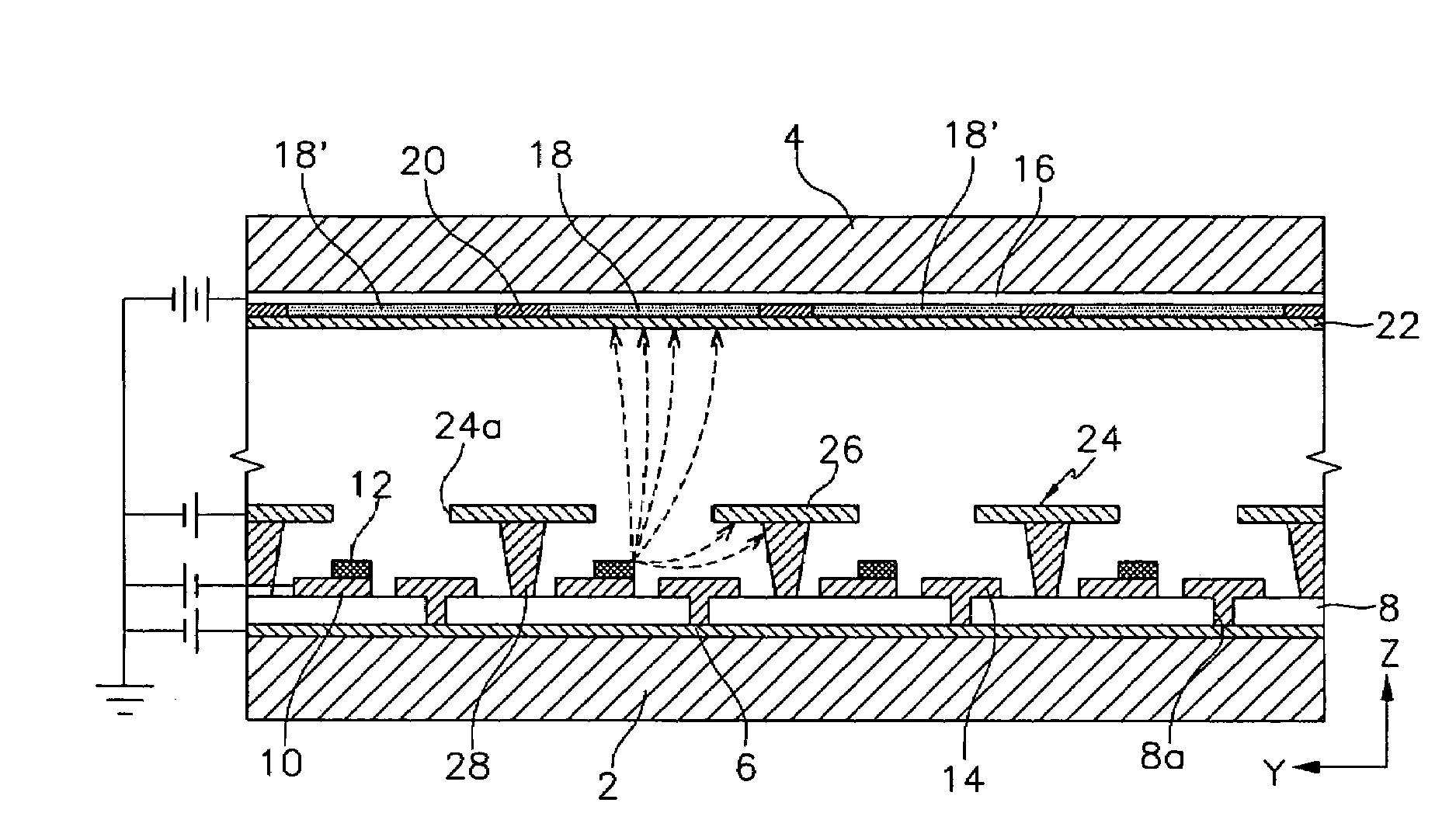
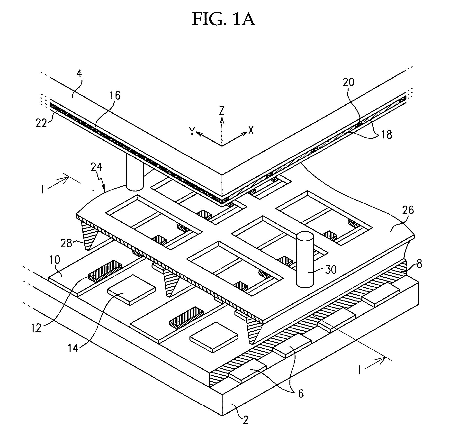
[0031]Referring to FIGS. 1A and 2, the FED includes first substrate 2 and second substrate 4 provided opposing one another with a predetermined gap therebetween. A structure to enable the emission of electrons by forming an electric field is provided on first substrate 2, and a structure to enable the realization of predetermined images by interaction with emitted electrons is provided on second substrate 4.

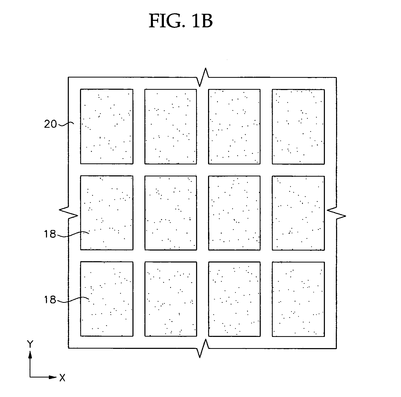
[0032]In more detail, gate electrodes 6 are formed on first substrate 2 in a stripe pattern along one direction (for example, axis Y direction of the drawings). Further, insulation layer 8 is formed over an entire surface of first substrate 2 covering gate electrodes 6. Cathode electrodes 10 are formed on insulation layer 8 in a stripe pattern along a direction perpendicular to the direction of long axes of gate electrodes 6 (for example, axis X direction of the drawings).

[0033]Pixel regions are defined by the intersection of gate electrodes 6 and cathode electrodes 10. Electron ...


PUM


Abstract

A field emission display including a first substrate and a second substrate opposing one another with a predetermined gap therebetween. An electron emission assembly is formed on the first substrate that emits electrons by the formation of an electric field. An illumination assembly is formed on the second substrate that realizes the display of images by the emitted electrons. A grid plate is mounted between the first and second substrates and functions to focus the emitted electrons. The grid plate includes a mask section having a plurality of apertures for passing the electrons, and supports mounted to one side of the mask section and extending in a direction toward the first substrate to rest on the same and support the mask section. The mask section and the supports are made of same material or two different materials.

Description

CROSS REFERENCE TO RELATED APPLICATION[0001]This application claims priority to and the benefit of Korea Patent Application No. 2003-0019225 filed on Mar. 27, 2003 in the Korean Intellectual Property Office, the entire content of which is incorporated herein by reference.BACKGROUND OF THE INVENTION[0002](a) Field of the Invention[0003]The present invention relates to a field emission display (FED), and more particularly, to an FED that includes emitters made of a carbon-based material and a grid plate mounted between front and rear substrates.[0004](b) Description of the Related Art[0005]In modern FEDs, a thick-layer process such as screen printing is used to form electron emission sources. The emission sources are formed using a carbon-based material that emits electrons at low voltage driving conditions of 10-100 V.[0006]Carbon-based materials suitable for forming the emitters include graphite, diamond, diamond-like carbon, and carbon nanotubes. Among these, carbon nanotubes appea...

Claims


Application Information

Patent Timeline
Patent Type & Authority Patents(United States)
IPC IPC(8): H01J63/02H01J1/62H01J1/88H01J19/42H01J1/30H01J1/46H01J21/10H01J29/46H01J29/48H01J31/12
CPCH01J29/467H01J29/481H01J31/127C01B32/05H01J1/30
Inventor CHI, EUNG-JOONJIN, SUNG-HWANJI, KWANG-SUN
Owner SAMSUNG SDI CO LTD
Why Eureka
Try Eureka