Image forming apparatus

a technology of image forming apparatus and forming nip, which is applied in the direction of electrographic process apparatus, instruments, optics, etc., can solve the problems of limiting the resolution of the increase, the “blank area” of the image defect, and the limited amount of toner present in the developing nip, so as to reduce the generation of the blank area of the imag

Inactive Publication Date: 2008-12-30
CANON KK
View PDF16 Cites 3 Cited by
  • Summary
  • Abstract
  • Description
  • Claims
  • Application Information

AI Technical Summary

Benefits of technology

[0026]An object of the present invention is to provide an image forming apparatus capable of reducing generation of a blank area of an image.
[0027]Another object of the present invention is to provide an image forming apparatus capable of reducing generation of an image defect of an interface between a high-density portion and a medium contrast portion.
[0028]Another object of the present invention is to provide an image forming apparatus capable of reducing charging failure caused by toner charges in a latent image potential during development.
[0029]Another object of the present invention is to provide an image forming apparatus capable of performing high-resolution image formation.

Problems solved by technology

In the case of the organic photoreceptor having a charge generation mechanism in an inner portion of the organic photoreceptor, charge diffusion occurs before charges reach a surface of the organic photoreceptor, so that there is a limit to an increase in resolution.
However, an image defect “blank area” generates unlike the case where the organic photoreceptor having the low capacitance is used.
A toner amount which is present in a developing nip is limited, so the toner amount necessary to sufficiently satisfy the development contrast voltage Vcont for the a-Si photosensitive member cannot be developed under the circumstances.
In particular, in order to fill the development contrast voltage Vcont on the high-density portion whose potential difference is large, an extremely large charge amount is necessary.
However, because the toner amount which is present in the developing nip and can be developed is limited, the development contrast voltage Vcont cannot be filled for the a-Si photosensitive member.
As a result, the “charging failure” occurs, so that the image defect called the “blank area” generates.
Therefore, as in the case of the a-Si photosensitive member, a high-capacitance organic photoreceptor whose capacitance is made equal to or larger than 1.7×10⁻⁶ (F / m2) by thin film processing has a problem in which the “charging failure” occurs, so that the image defect called the “blank area” generates.

Method used


Image

  • Image forming apparatus
  • Image forming apparatus
  • Image forming apparatus

Examples


embodiment 1

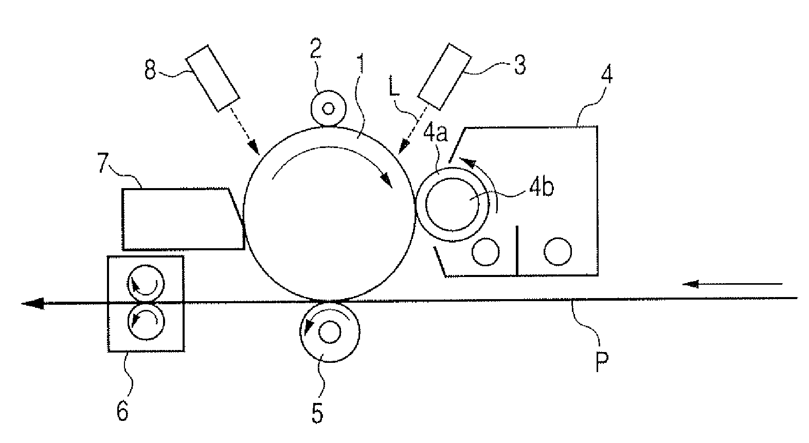
[0049](1) Schematic Structural Description of Image Forming Apparatus Example

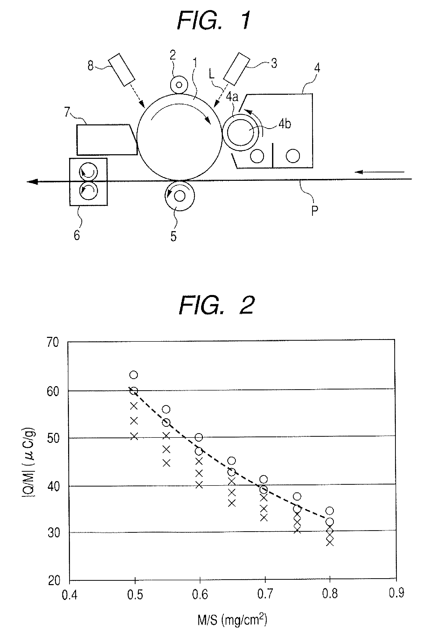
[0050]FIG. 1 is a schematic structural model view showing an image forming apparatus according to this embodiment. The image forming apparatus according to this embodiment is an electrophotographic laser printer using an amorphous silicon photosensitive member (a-Si photosensitive member) as an image bearing member. The a-Si photosensitive member is a photosensitive member of negative charge polarity. An image exposure system and a reverse developing system are employed and a resolution is 1200 dpi.

[0051]A drum-shaped a-Si photosensitive member 1 includes a photoconductive layer formed on an aluminum base 11. The photoconductive layer comprises an electron blocking layer 15, a charge generation layer 16, a hole blocking layer 17, and a surface layer as shown in FIG. 6. A thickness Ld of the photoconductive layer is 40 μm (=40×10−6 m) and a capacitance per unit area of the photoconductive layer is 2.2×10⁻⁶ (...

embodiment 2

[0190]In this embodiment, an example, in which a toner particle diameter is reduced in the structure described in Embodiment 1,will be described.

[0191]A background that the toner particle diameter is reduced is as follows. In order to output, as an electrophotography, a high-resolution image which surpasses other outputted images in a printing market, a method of reducing a laser spot diameter to obtain high resolution is employed. However, in order to more accurately visualize a high-resolution electrostatic latent image by a developing process, it is necessary that the toner particle diameter be small.

[0192]Therefore, in this embodiment, an example of an image forming apparatus whose resolution is 2400 dpi will be described.

[0193]In this embodiment, the exposure device 3 including a blue laser whose light emission wavelength is approximately 420 nm is used to obtain the resolution of 2400 dpi.

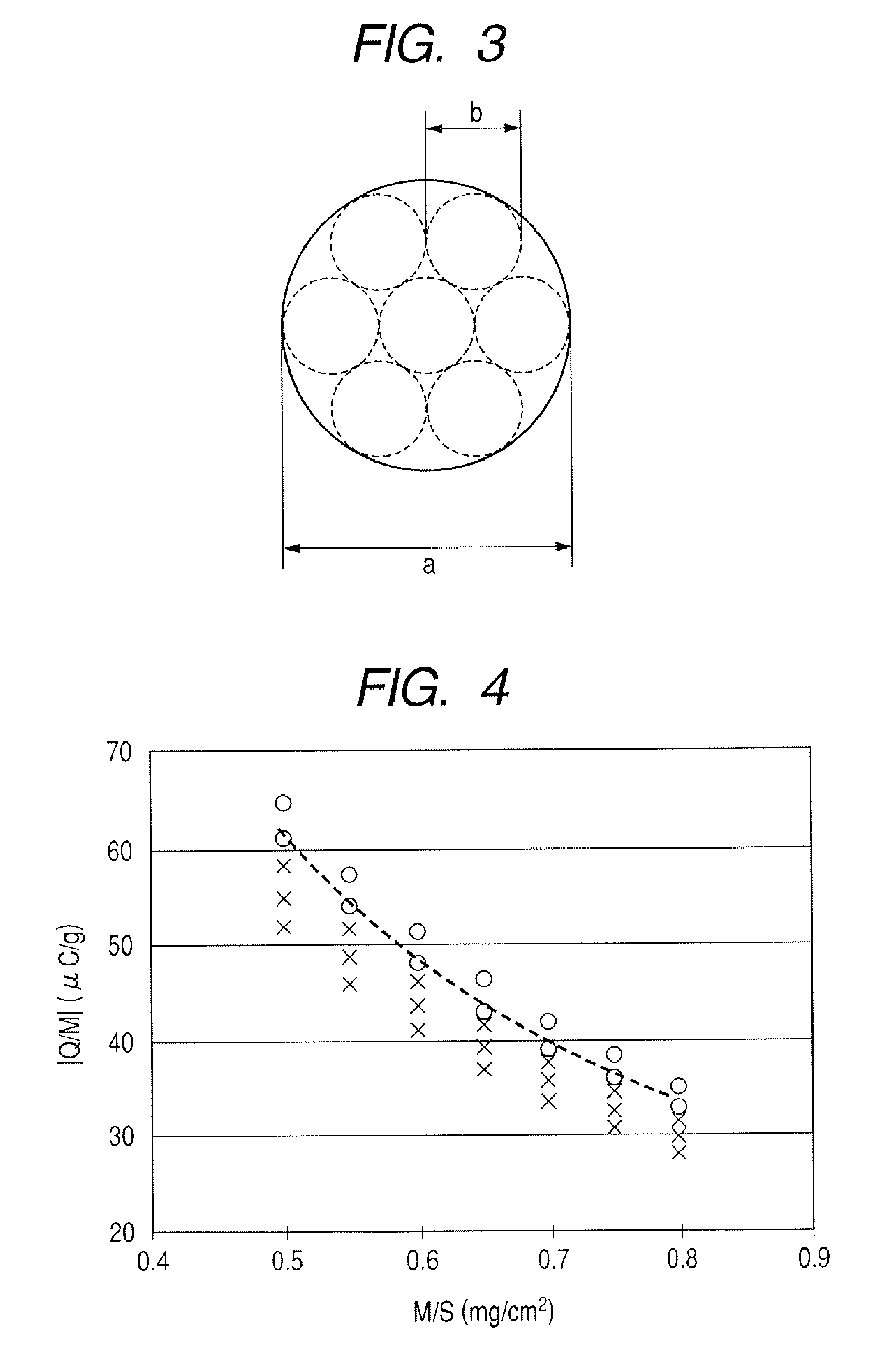
[0194]A spot diameter of 2400 dpi is approximately 10.6 μm. In order to more accurately v...


PUM


Abstract

An image forming apparatus including: an image bearing member having a photoconductive layer of a capacitance per unit area of 1.7×10⁻⁶ (F / m2) or more; and a developing device having a developer carrying member to which development voltage is applied for developing a latent image to form a toner image on the image bearing member, wherein the following expression is satisfied:QM≥0.95×Vcont(MS)×(Lt2⁢ɛ0⁢ɛt+Ldɛ0⁢ɛd)where Q / M (C / g): an electric charge quantity per unit weight of the toner image, Vcont: a potential difference between a surface potential of the image bearing member and a direct current component of the development voltage, M / S (g / m2): a toner weight per unit area of the maximum density portion, Lt (m): a toner layer thickness in the maximum density portion, Ld (m): a photoconductive layer thickness, εt: a relative permittivity of the toner layer, εd: a relative permittivity of the photoconductive layer, and ε0 (F / m): a vacuum permittivity.

Description

BACKGROUND OF THE INVENTION[0001]1. Field of the Invention[0002]The present invention relates to an image forming apparatus, such as a copying machine and a printer, for visualizing an electrostatic latent image formed on an image bearing member with toner to obtain an image.[0003]In particular, the present invention relates to an image forming apparatus in which a high-capacitance photoconductive layer whose capacitance per unit area is equal to or larger than 1.7×10⁻⁶ (F / m2) is used for the image bearing member.[0004]2. Description of the Related Art[0005]In general, in an electrophotographic image forming apparatus, an organic photoreceptor is widely used as a photosensitive member which is an image bearing member. FIG. 5 is a layer structural model view showing an example of the organic photoreceptor. In the organic photoreceptor, a charge generation layer 12 made of an organic material, a charge transport layer 13, and a surface protecting layer 14 are stacked on a metal base 1...

Claims


Application Information

Patent Timeline
Patent Type & Authority Patents(United States)
IPC IPC(8): G03G15/08
CPCG03G5/047G03G5/08214G03G15/0813G03G15/5037G03G15/751G03G15/5041G03G2215/0634
Inventor HARAGUCHI, MANAMIKUBO, KENTAYAMAMOTO, TAKESHI
Owner CANON KK
Why Eureka
Try Eureka