Thin film semiconductor device and fabrication method therefor

a technology of thin film semiconductors and fabrication methods, applied in semiconductor devices, semiconductor/solid-state device details, electrical devices, etc., can solve problems such as shallow contact holes, and achieve the effect of preventing an increase in the aspect ratio of contact holes

Inactive Publication Date: 2009-02-10
SHARP KK
View PDF21 Cites 217 Cited by
  • Summary
  • Abstract
  • Description
  • Claims
  • Application Information

AI Technical Summary

Benefits of technology

[0012]An object of the present invention is to provide a semiconductor device which can prevent an increase in an aspect ratio of a contact hole formed in an insulation layer in a region in which a transferred device is formed, the semiconductor device including a substrate on which (i) a transferred device which is a semiconductor device formed by transferring devices to an insulator substrate from a semiconductor substrate in which a part of device configuration has been incorporated, and (ii) a deposited device which is a semiconductor device formed on the insulator substrate whose semiconductor film is formed by a deposition process, coexist.
[0019]To meet the requirements, in the foregoing configuration, the contact hole is provided so as to be divided, by the relaying pad, into two parts, one extending upwards and the other extending downwards with respect to the relaying pad provided in the insulation layer, instead of forming the contact hole penetrating all of the insulation layer in the formation region of the transferred device. As such, the diameter of the contact hole can be made smaller than that of the contact hole penetrating all of the insulation layer without the relaying pad, thereby restraining the aspect ratio of the contact hole, and thereby reducing the size of the contact hall. This gives rise to an advantageous in high-density integration of circuits. Further, the contact hole becomes shallow. This allows reduction of the occurrences of problems such as connection failure of the connection wiring within the contact hole.

Problems solved by technology

Further, the contact hole becomes shallow.

Method used


Image

  • Thin film semiconductor device and fabrication method therefor
  • Thin film semiconductor device and fabrication method therefor
  • Thin film semiconductor device and fabrication method therefor

Examples


Embodiment Construction

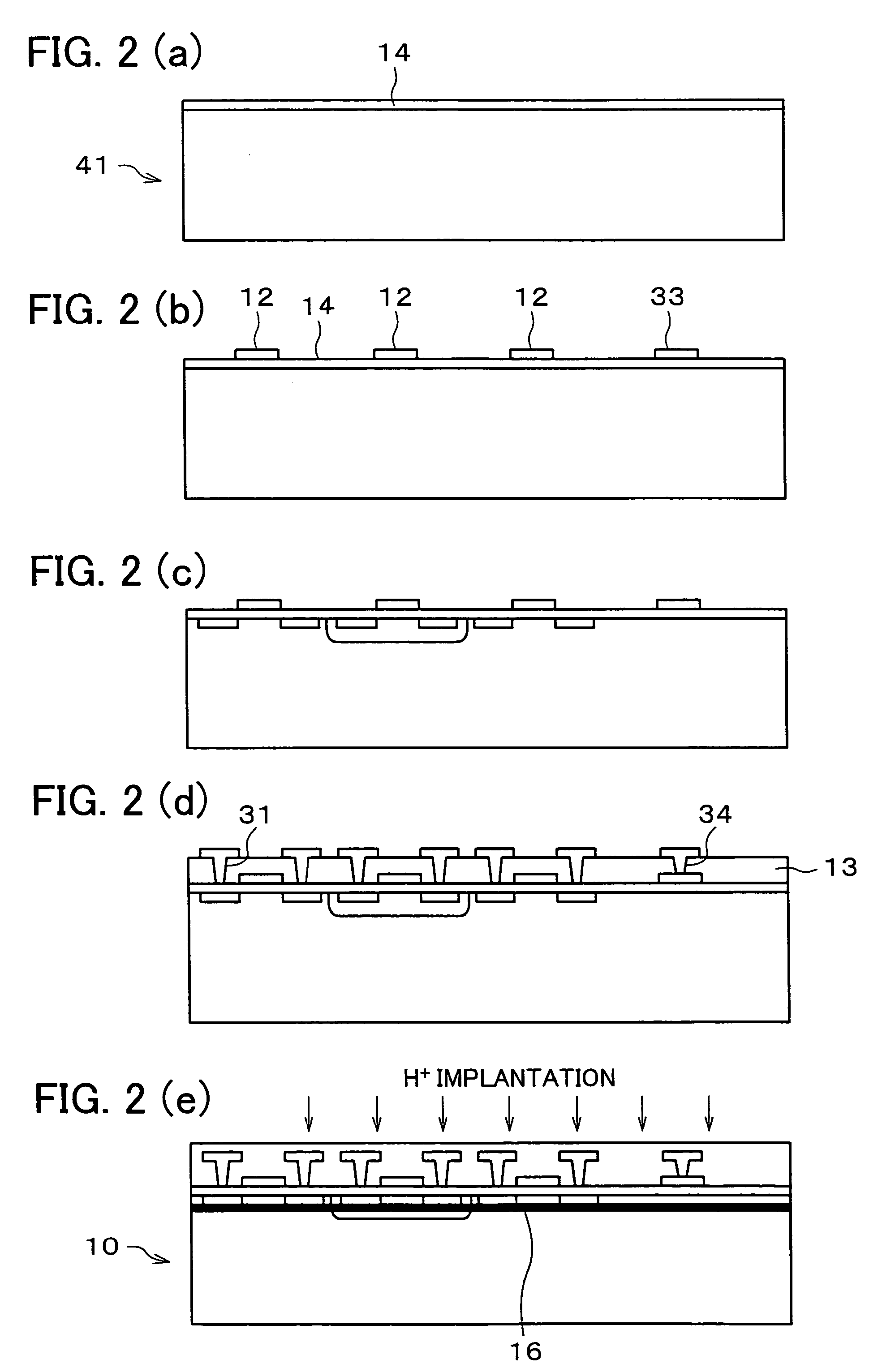
[0025]An embodiment in accordance with the present invention is described as follows with reference to drawings.

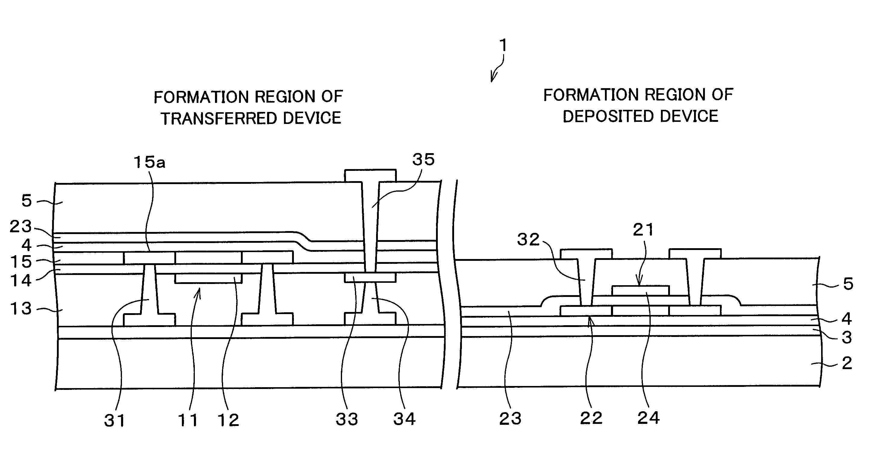
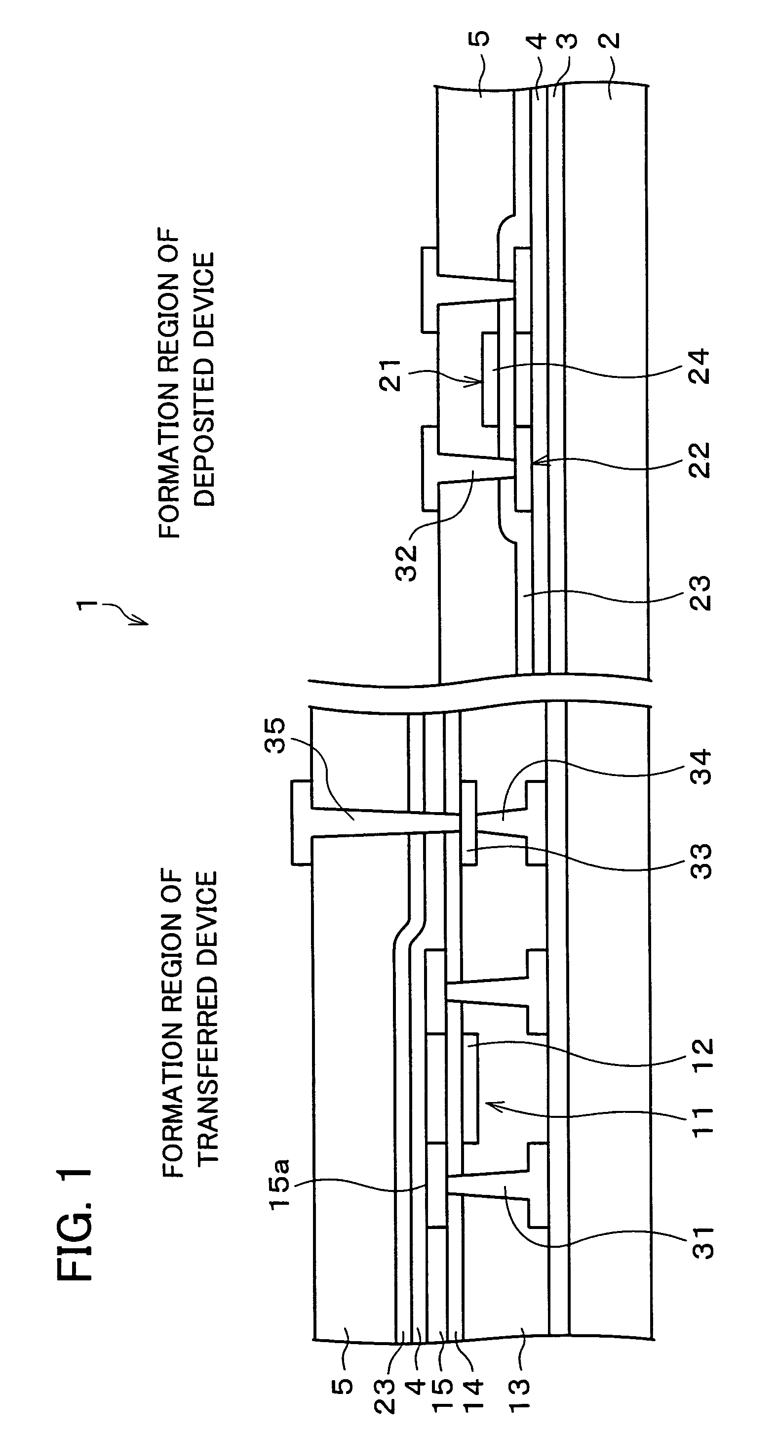
[0026]A thin film semiconductor device which the present embodiment deals with is a semiconductor device, suitable for high performance and high functionality, in which (i) a MOS non-single-crystal silicon thin film transistor, and (ii) a MOS single-crystal silicon thin film transistor are provided in different regions on an insulator substrate. Such semiconductor device is arranged on an active matrix substrate using TFTs (thin film transistors).

[0027]This MOS thin film transistor is a popular transistor including an active semiconductor layer, a gate electrode, a gate insulation layer, and a highly-concentrated impurity doped sections (source electrode, and drain electrode) provided on both sides of the gate. In such a MOS thin film transistor, carrier concentration of the semiconductor layer below the gate is modulated in accordance with a voltage applied to the gate el...


PUM


Abstract

A relaying pad is formed in a predetermined portion in an insulation layer of the single-crystal thin film device, in a region where the single-crystal thin film device is formed. The relaying pad is for providing connection wiring through the insulator substrate. With this configuration it is possible to prevent an increase in an aspect ratio of a contact hole formed in an insulation layer in a region in which a transferred device is formed, the semiconductor device including a substrate on which the transferred device and a deposited device coexist.

Description

[0001]This Nonprovisional application claims priority under 35 U.S.C. § 119(a) on Patent Application No. 2003 / 325781 filed in Japan on Sep. 18, 2003, the entire contents of which are hereby incorporated by reference.FIELD OF THE INVENTION[0002]The present invention relates to a thin film semiconductor device and a fabrication method therefor for used in, for example, a liquid crystal display device which is driven by TFTs in an active matrix manner. The present invention is for improving a circuit performance in such a liquid crystal display device in which a peripheral driving circuit, a control circuit, and other circuits are integral with each other and are integrated into a single substrate.BACKGROUND OF THE INVENTION[0003]A display device in which a liquid crystal panel or an organic EL (electro luminescent) panel is driven by thin film transistors (hereinafter referred to as TFTs) in so-called an active matrix manner has been used recently. In such a display device, there is p...

Claims


Application Information

Patent Timeline
Patent Type & Authority Patents(United States)
IPC IPC(8): H01L29/04H01L27/01H01L27/12H01L31/036H01L31/0392H01L21/02H01L23/522H01L21/336H01L21/762H01L21/768H01L21/77H01L21/84H01L23/52H01L29/786
CPCH01L21/76254H01L21/76897H01L27/124H01L27/1266H01L29/66757H01L29/66772H01L2924/1305H01L2924/13091H01L2221/68363H01L2224/24226H01L2924/01021H01L2924/00H01L27/12H01L27/1214
Inventor TAKAFUJI, YUTAKAITOGA, TAKASHIOGAWA, YASUYUKI
Owner SHARP KK
Why Eureka
Try Eureka