Semiconductor device including metal-oxide-silicon field-effect transistor as a trigger circuit

a metal-oxide-silicon and trigger circuit technology, applied in semiconductor devices, semiconductor/solid-state device details, electrical equipment, etc., can solve the problems of high trigger voltage of scr, easy damage to the internal circuit of the semiconductor integrated circuit, and easy application of destructive stress

Inactive Publication Date: 2009-01-06
KK TOSHIBA
View PDF6 Cites 9 Cited by
  • Summary
  • Abstract
  • Description
  • Claims
  • Application Information

AI Technical Summary

Problems solved by technology

On the other hand, the SCR has the disadvantage that its trigger voltage is high.
If the trigger voltage is high, the internal circuit of the semiconductor integrated circuit is easily subjected to electrostatic discharge damage.
The application of an ESD surge causes a destructive stress to be applied to the gate insulation films of the elements in the internal circuit, or it causes the elements in the internal circuit to turn on earlier than the SCR and causes a destructive current to flow through a circuit board.
However, it is difficult to control the breakdown voltage at the PN junction and drop the trigger voltage to a fixed level or lower.
The device disclosed in the above publication, in which the trigger voltage Vt1 takes on discontinuous values only, is unsuitable to design an ESD protection circuit device.
A large leakage current occurs accordingly.
To achieve this, a very large circuit area is required.
It was therefore difficult to achieve a high-performance semiconductor integrated circuit inexpensively.

Method used


Image

  • Semiconductor device including metal-oxide-silicon field-effect transistor as a trigger circuit
  • Semiconductor device including metal-oxide-silicon field-effect transistor as a trigger circuit
  • Semiconductor device including metal-oxide-silicon field-effect transistor as a trigger circuit

Examples


first embodiment

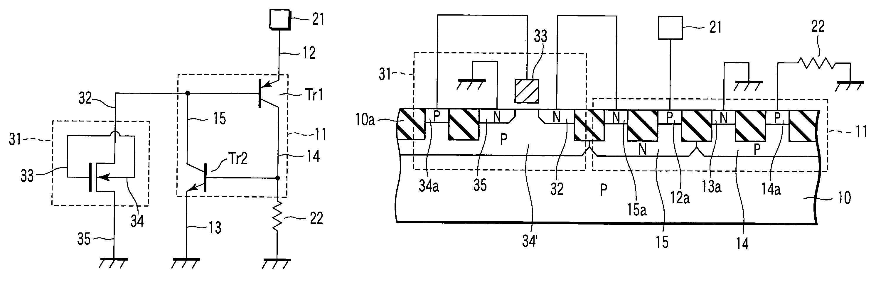
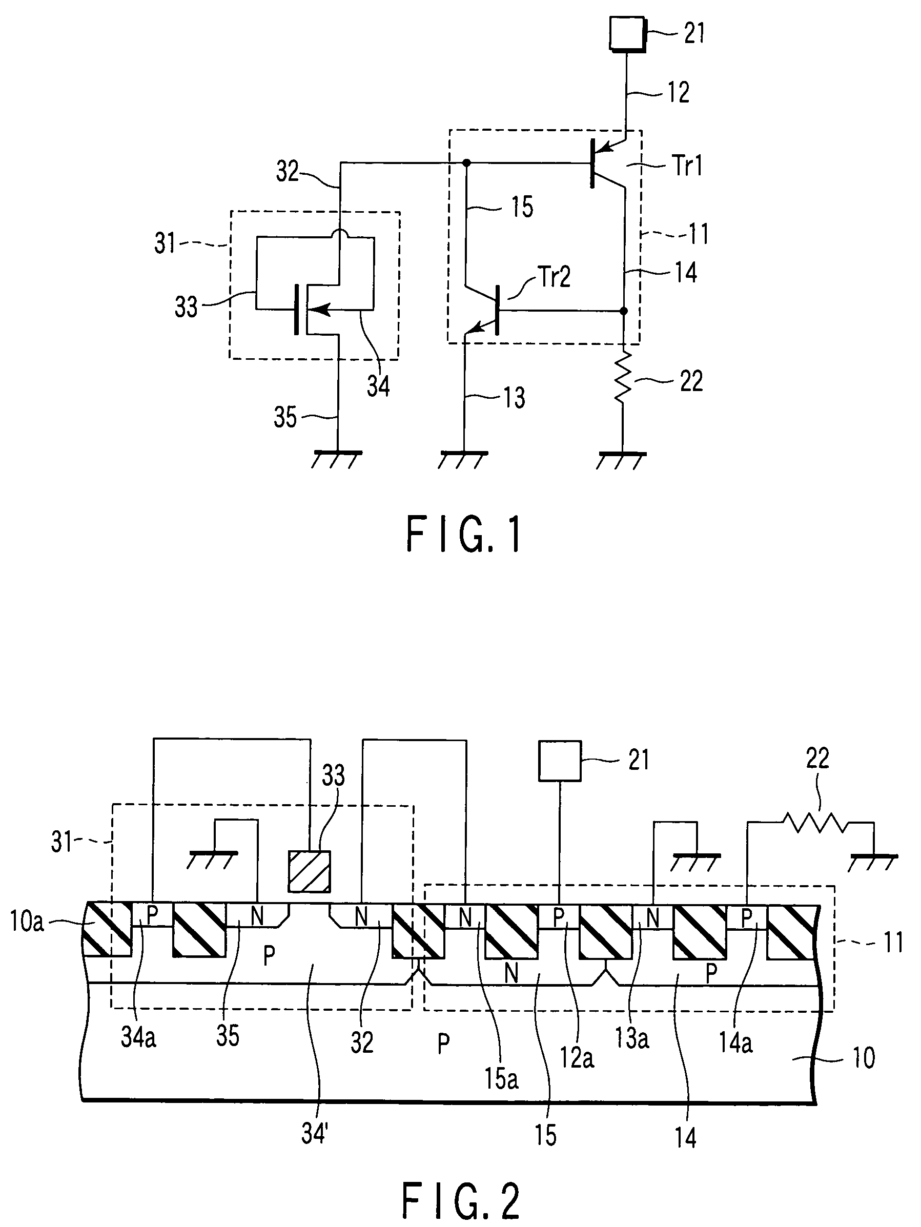
[0028]FIG. 1 shows a basic configuration of an ESD protection circuit device according to a first embodiment of the present invention, which is used in a semiconductor integrated circuit. The ESD protection circuit device is of an SCR type and has a first MOSFET as a trigger circuit. In this device, the MOSFET and SCR are loaded onto a p-type semiconductor substrate (Si substrate).

[0029]Referring to FIG. 1, the SCR 11 has an anode (emitter of PNP transistor Tr1) 12 that is connected to a terminal 21. The terminal 21 is connected to an internal circuit (e.g., a power line and an input / output signal line) of a semiconductor integrated circuit (not shown). The SCR 11 also has a cathode (emitter of NPN transistor Tr2) 13 that is grounded via a power line or the like. Further, the SCR 11 has a P well region (collector of PNP transistor Tr1 and base of NPN transistor Tr2) 14 that is grounded via a resistance element (external resistor) 22 whose resistance value is about 1 KΩ.

[0030]The SCR...

second embodiment

[0044]FIG. 5 shows a basic configuration of an ESD protection circuit device according to a second embodiment of the present invention, which is used in a semiconductor integrated circuit. The ESD protection circuit device is of an SCR type and has a MOSFET as a trigger circuit. This device is configured to suppress a leakage current in normal circuit operation. The same components as those of FIG. 1 are indicated by the same reference numerals and their detailed descriptions are omitted.

[0045]Referring to FIG. 5, an SCR 11 has an anode (emitter of PNP transistor Tr1) 12 that is connected to a terminal 21. The terminal 21 is connected to an internal circuit (e.g., a power line and an input / output signal line) of a semiconductor integrated circuit (not shown). The SCR 11 also has a cathode (emitter of NPN transistor Tr2) 13 that is grounded via a power line or the like. Further, the SCR 11 has a P well region (collector of PNP transistor Tr1 and base of NPN transistor Tr2) 14 that is...


PUM


Abstract

A semiconductor device includes a silicon-controlled rectifier to protect an internal circuit from electrostatic discharge damage and a first metal-oxide-silicon field-effect transistor to apply a trigger voltage to the silicon-controlled rectifier. The first metal-oxide-silicon field-effect transistor including a gate electrode and a substrate which are electrically connected to each other.

Description

CROSS-REFERENCE TO RELATED APPLICATIONS[0001]This application is based upon and claims the benefit of priority from prior Japanese Patent Application No. 2005-132094, filed Apr. 28, 2005, the entire contents of which are incorporated herein by reference.BACKGROUND OF THE INVENTION[0002]1. Field of the Invention[0003]The present invention relates to a semiconductor device. More specifically, the invention relates to an electrostatic discharge (ESD) protection circuit device of a silicon-controlled rectifier (SCR) type, which has a metal-oxide-silicon field-effect transistor (MOSFET) as a trigger circuit and is used in a semiconductor integrated circuit.[0004]2. Description of the Related Art[0005]As is well known, it is essential to make practical use of an SCR to protect a semiconductor integrated circuit (or its internal circuit) from ESD. The SCR has the advantage that its on-resistance is extremely low. The SCR is thus suitable to protect a gate insulation film that is thinned by...

Claims


Application Information

Patent Timeline
Patent Type & Authority Patents(United States)
IPC IPC(8): H01L27/12
CPCH01L27/0262H01L2924/0002H01L2924/00
Inventor KONDO, MASAKI
Owner KK TOSHIBA
Why Eureka
Try Eureka