Gallium nitride-based semiconductor light emitting device and process for its production
a technology of gallium nitride and light emitting device, which is applied in the manufacture of semiconductor/solid-state devices, semiconductor devices, electrical equipment, etc., can solve the problems of affecting the light emission output of the light emitting device. , to achieve the effect of avoiding shorting of the light emitting device, reducing light emission output, and high light reflectivity
- Summary
- Abstract
- Description
- Claims
- Application Information
AI Technical Summary
Benefits of technology
Problems solved by technology
Method used
Image
Examples
example 1
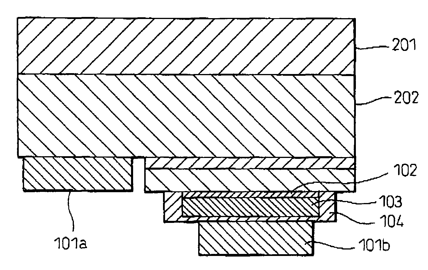
[0059]Using a sapphire (Al2O3) C-surface substrate as the substrate, there were laminated thereover an undoped GaN layer to 6 μm and an n-type contact layer periodically doped with Ge to a mean carrier concentration of 1×1019 cm−3 to 4 μm, and five times in an alternating fashion a 12.5 nm n-clad layer made of In0.1Ga0.9N, a 16 nm-thick barrier layer made of GaN and a 2.5 nm-thick well layer made of In0.2Ga0.8N, via an AlN buffer according to the method disclosed in Japanese Unexamined Patent Publication No. 2003-243302, and then finally a luminescent layer having a multiple quantum well structure provided with barrier layer, a 0.05 μm-thick p-clad layer composed of Mg-doped (8×10¹⁹ / cm3 concentration) Al0.2Ga0.8N and a 0.15 μm-thick p-contact layer composed of Mg-doped (8×10¹⁹ / cm3 concentration) Al0.03Ga0.97N were laminated in that order to obtain a nitride semiconductor layer on the substrate.
[0060]Publicly known lithography and Cl2 gas RIE were used to expose the individual elemen...
example 2
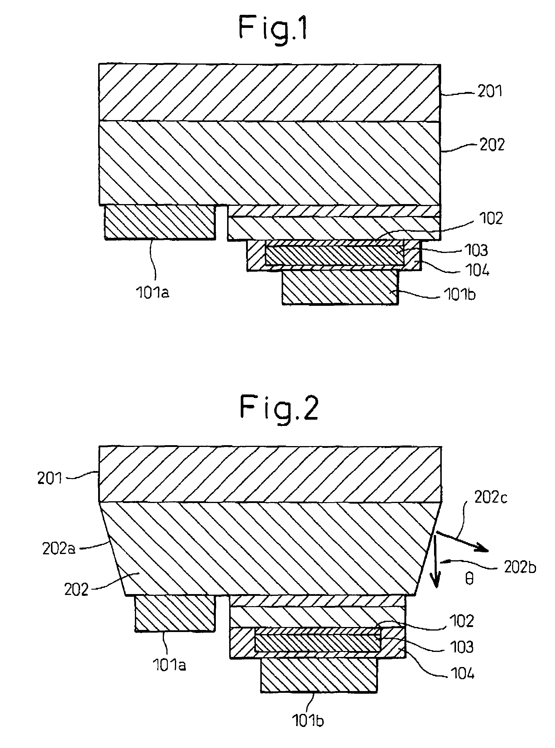
[0067]This is an example of forming an inclination surface on the semiconductor side surfaces. Although an inclination surface with a positive angle was formed on the semiconductor side surfaces in this example, the same effect is achieved if the inclination surface has a negative angle.
[0068]The inclination surface was formed by dry etching. First, the individual element boundary sections and n-type contact layer sections were exposed under the same conditions as in Example 1. The etching depth was 0.8 μm. After removal of the resist, the resist was reapplied and lithography was performed to expose only the boundary sections. Etching was performed to 8 μm for a longer etching time than the first etching, for removal almost to the substrate. Because of the extended time, receding of the resist was no longer negligible, and as it disappeared from the edges a natural inclination surface was formed on the etching surface, The inclination angle θ was 50°-60°.
[0069]After releasing the re...
PUM
 Abstract
Description
Claims
Application Information

