Gallium nitride-based semiconductor light emitting device and process for its production

Active Publication Date: 2007-03-15
TOYODA GOSEI CO LTD
View PDF4 Cites 28 Cited by
  • Summary
  • Abstract
  • Description
  • Claims
  • Application Information

AI Technical Summary

Benefits of technology

[0034] Since the present invention includes a reflective layer containing Ag in the p-type electrode of a light emitting device that extracts light from the sides of the substrate, the light reflectivity is high. Furthermore, since the reflective layer is covered with a prote

Problems solved by technology

However, Ag metal is also known to be prone to electromigration, and electrodes with exposed Ag electrode sections inevitably suffer reduction in light emission output and deterioration in current-voltage characteristics due to shorting of the electrified elements.
Ideally, if the surface of the Ag electrode is completely covered in a protected electrode employing a separate metal it should be possible to prevent deterioration of the element characteristics,

Method used


Image

  • Gallium nitride-based semiconductor light emitting device and process for its production
  • Gallium nitride-based semiconductor light emitting device and process for its production

Examples


example 1

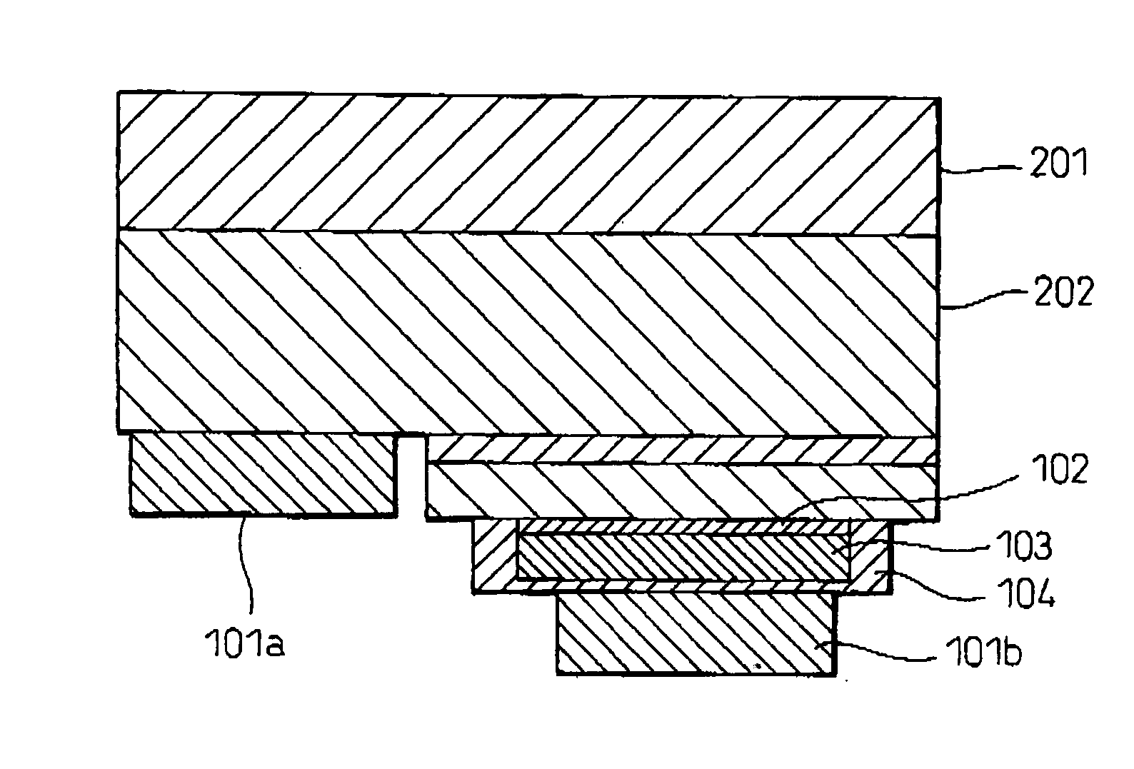
[0059] Using a sapphire (Al2O3) C-surface substrate as the substrate, there were laminated thereover an undoped GaN layer to 6 μm and an n-type contact layer periodically doped with Ge to a mean carrier concentration of 1×1019 cm−3 to 4 μm, and five times in an alternating fashion a 12.5 nm n-clad layer made of In0.1Ga0.9N, a 16 nm-thick barrier layer made of GaN and a 2.5 nm-thick well layer made of In0.2Ga0.8N, via an AlN buffer according to the method disclosed in Japanese Unexamined Patent Publication No. 2003-243302, and then finally a luminescent layer having a multiple quantum well structure provided with barrier layer, a 0.05 μm-thick p-clad layer composed of Mg-doped (8×10¹⁹ / cm3 concentration) Al0.2Ga0.8N and a 0.15 μm-thick p-contact layer composed of Mg-doped (8×10¹⁹ / cm3 concentration) Al0.03Ga0.97N were laminated in that order to obtain a nitride semiconductor layer on the substrate.

[0060] Publicly known lithography and Cl2 gas RIE were used to expose the individual ele...

example 2

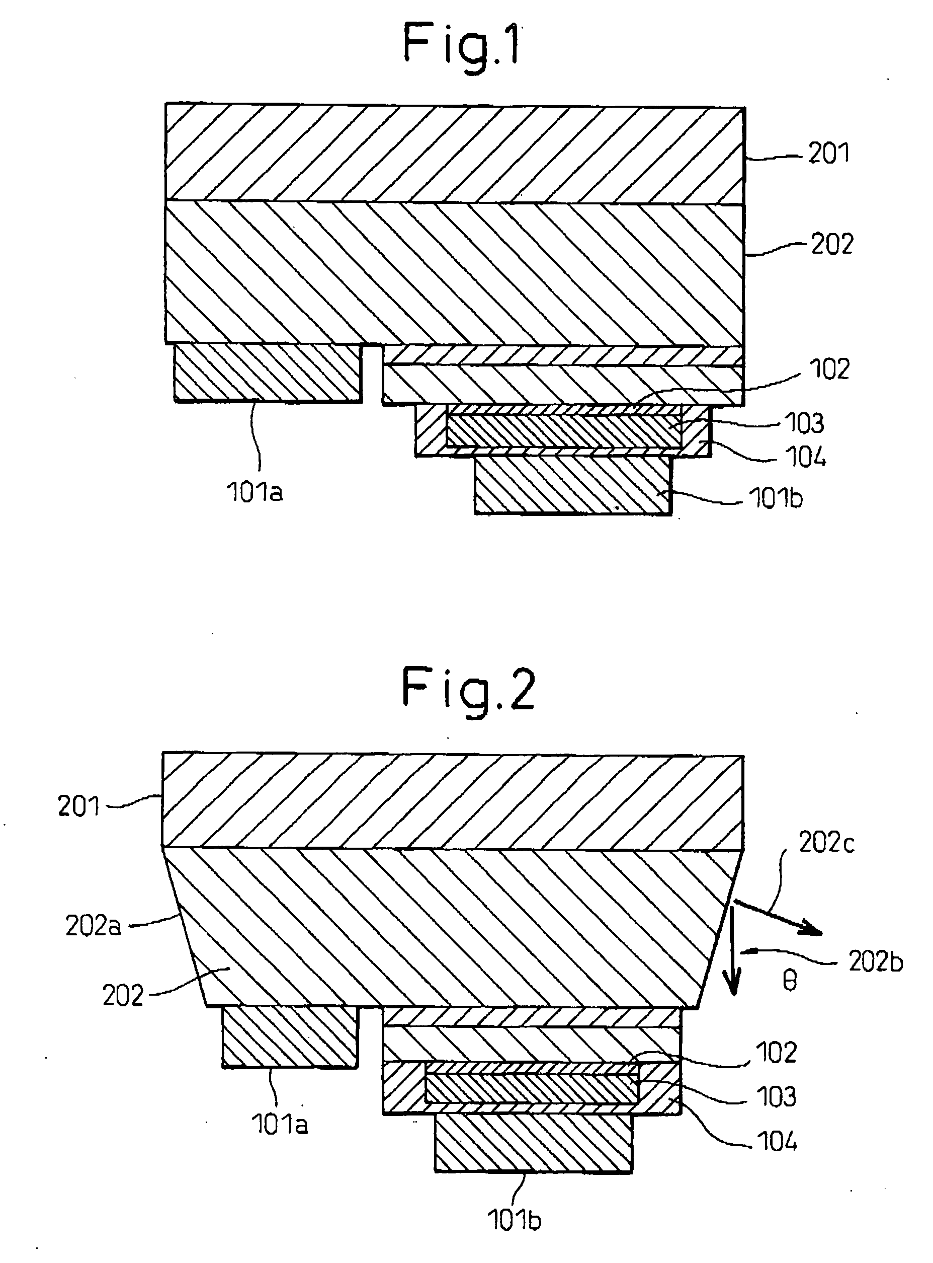
[0067] This is an example of forming an inclination surface on the semiconductor side surfaces. Although an inclination surface with a positive angle was formed on the semiconductor side surfaces in this example, the same effect is achieved if the inclination surface has a negative angle.

[0068] The inclination surface was formed by dry etching. First, the individual element boundary sections and n-type contact layer sections were exposed under the same conditions as in Example 1. The etching depth was 0.8 μm. After removal of the resist, the resist was reapplied and lithography was performed to expose only the boundary sections. Etching was performed to 8 μm for a longer etching time than the first etching, for removal almost to the substrate. Because of the extended time, receding of the resist was no longer negligible, and as it disappeared from the edges a natural inclination surface was formed on the etching surface, The inclination angle θ was 50°-60°.

[0069] After releasing t...


PUM


Abstract

It is an object of the present invention to inhibit exposure of Ag in Ag-employing reflective electrodes caused by microdefects generated during the manufacturing process, and to prevent reduction in light emission output and deterioration in current-voltage characteristics resulting from shorting of the light emitting device. The semiconductor light emitting device comprises an n-type semiconductor layer, a light emitting layer and a p-type semiconductor layer in that order on a substrate, with a negative electrode and positive electrode each formed in contact with the n-type semiconductor layer and p-type semiconductor layer, respectively. The positive electrode comprises at least a contact metal layer composed of at least one type of metal selected from the group consisting of Pt, Ir, Rh, Pd, Ru and Re or their alloy in contact with the p-type semiconductor layer, a reflective layer composed of a metal or alloy containing Ag as the main component on the contact layer, and one or more protective metal layers containing no Ag, covering the top and side surfaces of the reflective layer.

Description

CROSS REFERENCE TO RELATED APPLICATIONS [0001] This application claims benefit of Provisional Application Ser. No. 60 / 718,332 filed Sep. 20, 2005, incorporated herein by reference, under 35 U.S.C. 111(b) pursuant to 35 U.S.C. 119(e)(1).BACKGROUND OF THE INVENTION [0002] 1. Field of the Invention [0003] The present invention relates to a gallium nitride-based semiconductor light emitting device, and particularly to a gallium nitride-based semiconductor light emitting device which employs Ag in the electrode for increased light reflectivity, while preventing migration of Ag and exhibiting increased reliability as a light emitting diode. [0004] 2. Description of the Related Art [0005] Group III nitride semiconductors such as gallium nitride have a direct band gap of energy corresponding from the visible light range to the ultraviolet range and are capable of high efficiency luminosity, and therefore they are used in products such as light emitting diodes (LED) and laser diodes (LD). In...

Claims


Application Information

Patent Timeline
IPC IPC(8): H01L33/00H01L33/32H01L33/40
CPCH01L33/405H01L33/32
Inventor URASHIMA, YASUHITO
Owner TOYODA GOSEI CO LTD
Why Eureka
Try Eureka