Multiple quantum well semiconductor light emitting element

a light-emitting element and quantum well technology, applied in semiconductor lasers, semiconductor devices, laser details, etc., can solve the problems of reducing reducing the recombination efficiency between electrons and holes, increasing the probability of carrier trapping, etc., to reduce the recombination efficiency, and reduce the light emission output

Active Publication Date: 2015-05-14
STANLEY ELECTRIC CO LTD
View PDF1 Cites 3 Cited by
  • Summary
  • Abstract
  • Description
  • Claims
  • Application Information

AI Technical Summary

Benefits of technology

[0007]In general, when an operating temperature of a semiconductor light emitting element such as an LED is increased, a light emission output thereof is reduced. Such a reduction in light emission output is caused by a reduction in recombination efficiency between electrons and holes due to the overflow of carriers, an increased probability of carrier trapping due to defects in crystals, a reduced carrier injection efficiency, and the like.
[0008]There is a need for a semiconductor light emitting element capable of suppressing a reduction in the light emission efficiency thereof due to such physical phenomena and therefore maintaining the high light emission efficiency and also capable of achieving excellent temperature characteristics, i.e., the light emission efficiency and light emission output thereof being less likely to decrease even during a high-temperature operation thereof.
[0009]The present invention relates to a semiconductor light emitting element such as an LED or LD (laser diode) with the use of an MQW light emitting layer. It is an object of the present invention to provide a semiconductor light emitting element which can suppress the overflow of carriers and thus have a high carrier injection efficiency into the light emitting layer and which has a high light emission efficiency and excellent temperature characteristics.

Problems solved by technology

Such a reduction in light emission output is caused by a reduction in recombination efficiency between electrons and holes due to the overflow of carriers, an increased probability of carrier trapping due to defects in crystals, a reduced carrier injection efficiency, and the like.

Method used


Image

  • Multiple quantum well semiconductor light emitting element
  • Multiple quantum well semiconductor light emitting element
  • Multiple quantum well semiconductor light emitting element

Examples


example 1

[0034]Example 1 of the present invention will now be described below. Although a case where a semiconductor structure layer 10 as Example 1 is made of a GaN (gallium nitride)-based semiconductor will be described, the crystal system thereof is not limited thereto. More specifically, an LED was manufactured with the use of the semiconductor structure layer 10 and the light emission characteristics thereof were evaluated.

[0035]A circular sapphire monocrystalline substrate having a diameter of 2 inches and having a c-plane as the front surface thereof was employed as a crystal growth substrate. The semiconductor structure layer 10, which is an LED structure layer, was grown on the substrate by metal organic chemical vapor deposition (MOCVD).

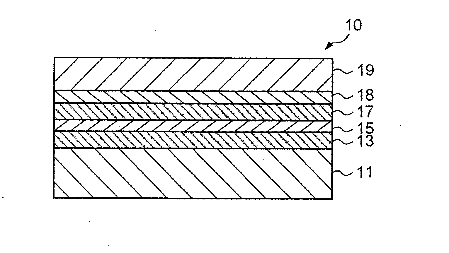
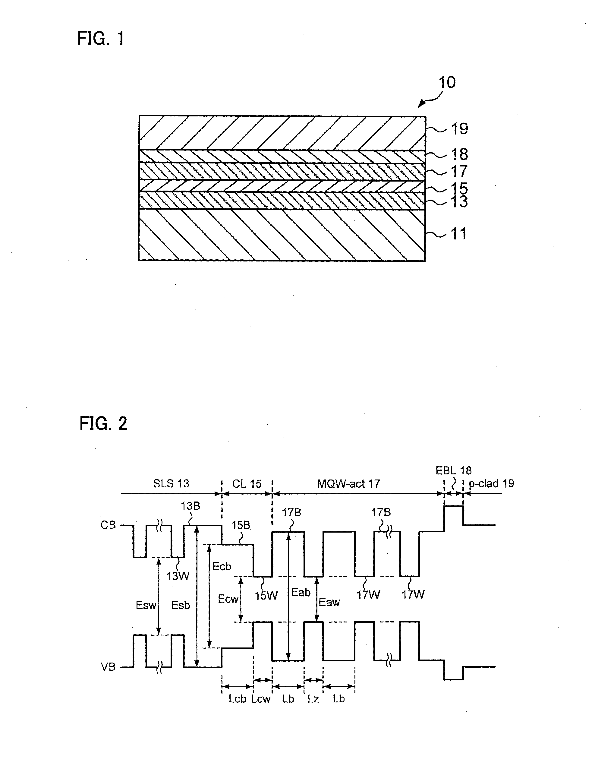
[0036]After growing a low-temperature GaN buffer layer, the semiconductor structure layer 10 was grown thereon. The semiconductor structure layer 10 has a structure including an n-GaN layer 11, an SLS layer 13, an electron injection control layer 15...


PUM


Abstract

A semiconductor light emitting element includes: an n-type semiconductor layer; a super lattice structure layer formed on the n-type semiconductor layer and including repeatedly-formed first semiconductor layers and second semiconductor layers having a composition with a band gap greater than that of the first semiconductor layer; an electron injection control layer including a first control layer formed on the second semiconductor layer of super lattice structure layer and a second control layer formed on the first control layer; and an MQW light emitting layer formed on the second control layer and including repeatedly-formed barrier layers and quantum well layers. The first control layer has a composition with a band gap smaller than that of the second semiconductor layer of super lattice structure layer. The second control layer has a composition and a thickness same as or smaller than those of the quantum well layer of the MQW light emitting layer.

Description

BACKGROUND OF THE INVENTION[0001]1. Field of the Invention[0002]The present invention relates to a semiconductor light emitting element having a light emitting layer with a multiple quantum well (MQW) structure. In particular, the present invention relates to a light emitting diode (LED) having an MQW light emitting layer.[0003]2. Description of the Related Art[0004]It has been known that the MQW structure can be employed in a light emitting layer in order to improve light emission characteristics such as light emission efficiency in a semiconductor light emitting element such as an LED or a semiconductor laser.[0005]Patent documents such as Japanese Patent Application Laid-Open No. Hei. 10-242512, Japanese Patent No. 4441563, Japanese Patent No. 4206086, Japanese Patent No. 4161603, and Japanese Patent Application Laid-Open No. 2002-176198 disclose various structures such as MQW layers or guide layers for improving light emission characteristics.SUMMARY OF THE INVENTION[0006]LEDs u...

Claims


Application Information

Patent Timeline
Patent Type & Authority Applications(United States)
IPC IPC(8): H01L33/00H01L33/32H01S5/343H01L33/06
CPCH01L33/0025H01S5/34333H01L33/325H01L33/06H01S5/2009H01S5/3216
Inventor YAMANE, TAKAYOSHI
Owner STANLEY ELECTRIC CO LTD
Why Eureka
Try Eureka