Scanned memory testing of multi-port memory arrays

a multi-port memory and array technology, applied in the field of asic design and manufacturability, can solve the problems of complex process to test the characteristics of memory array cells, difficult to achieve, and test multi-port memory

Active Publication Date: 2009-03-17
INT BUSINESS MASCH CORP
View PDF19 Cites 8 Cited by
  • Summary
  • Abstract
  • Description
  • Claims
  • Application Information

AI Technical Summary

Benefits of technology

[0005]The present invention addresses the above issues by providing mechanisms for scanned memory testing that use functional data latches from one port as shadow latches for another port during ABIST testing to achieve functional speed testing of multi-ported memories.

Problems solved by technology

Testing multi-port memory (e.g., Processor internal Register Memory Array) may present complications, such as how to fully test port interactions without necessitating large amounts of extra test-only hardware.
In addition, the AVP is generally developed late in the design process, typically after the hardware is developed, and it is a complex process to test memory array cell characteristics.
Since creating and maintaining such AVP programs can be labor-intensive and burdensome, it is difficult to accomplish this late in the design process without causing schedule or quality slippage.

Method used


Image

  • Scanned memory testing of multi-port memory arrays
  • Scanned memory testing of multi-port memory arrays
  • Scanned memory testing of multi-port memory arrays

Examples


Embodiment Construction

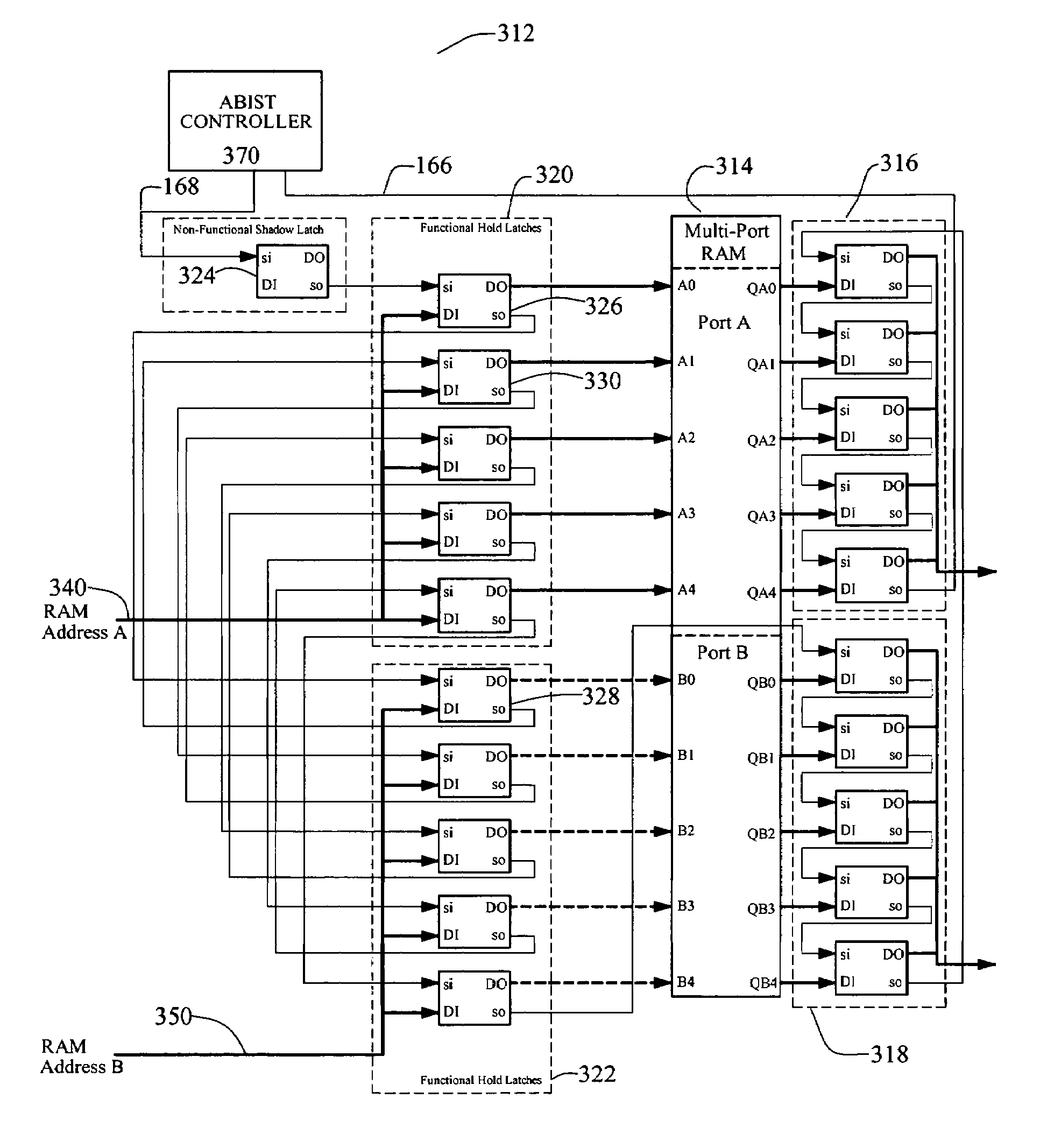
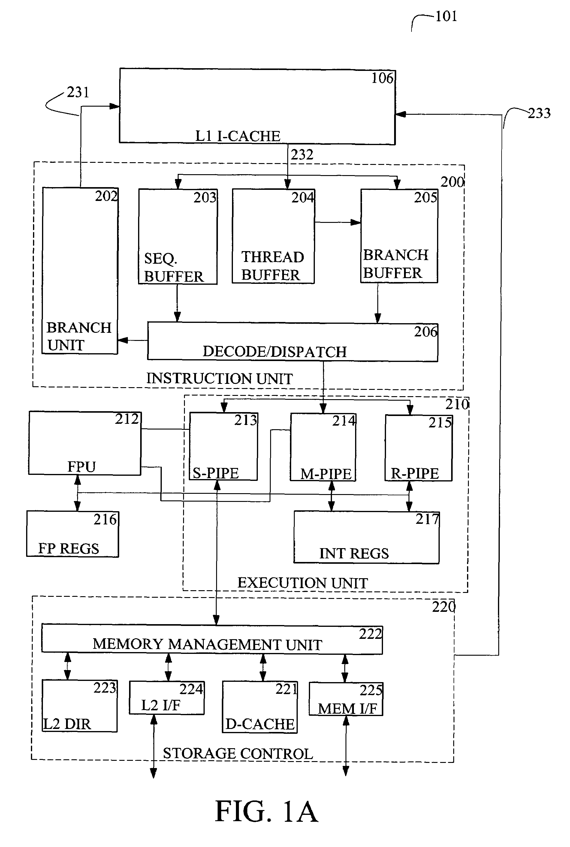
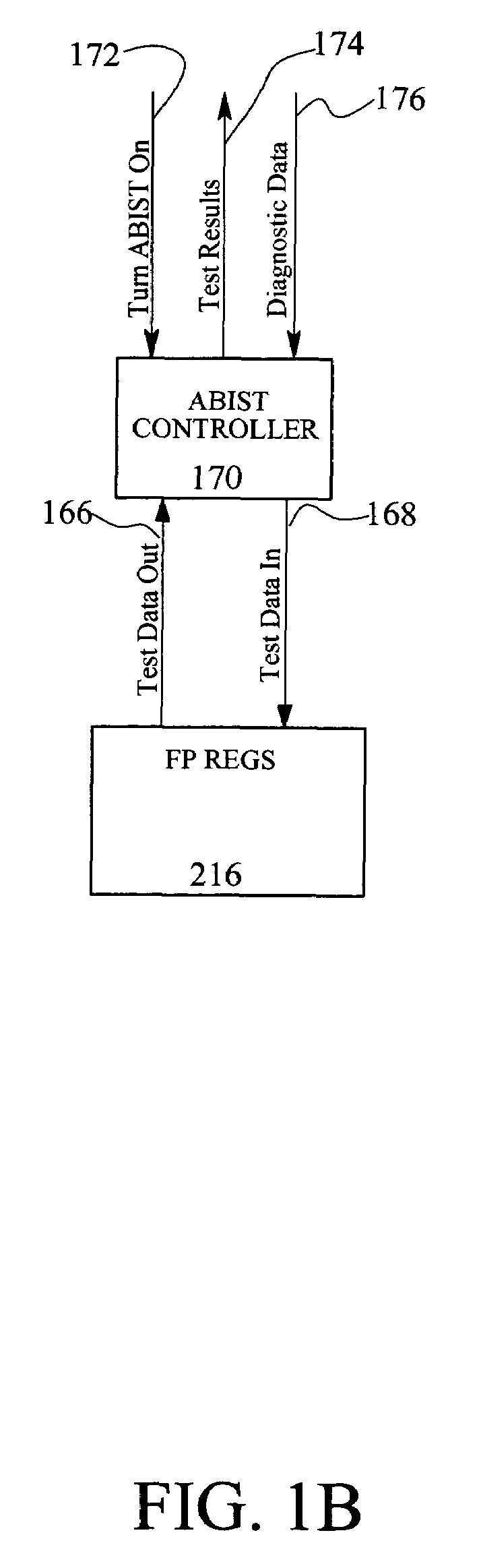
[0014]In the following description, numerous specific details are set forth such as specific data bit lengths, address lengths, widths of data lines, and array sizes, etc. to provide a thorough understanding of the present invention. However, it will be obvious to those skilled in the art that the present invention may be practiced without such specific details. In other instances, well-known circuits have been shown in block diagram form in order not to obscure the present invention in unnecessary detail. Some details concerning timing considerations, detection logic, specific ABIST software code and the like have been omitted inasmuch as such details are not necessary to obtain a complete understanding of the present invention and are within the skills of persons of ordinary skill in the relevant art. Refer now to the drawings wherein depicted elements are not necessarily shown to scale and like or similar elements may be designated by the same reference numeral through the severa...


PUM


Abstract

A system for at-functional-clock-speed continuous scan array built-in self testing (ABIST) of multiport memory is disclosed. During ABIST testing, functional addressing latches from a first port are used as shadow latches for a second port's addressing latches. The arrangement reduces the amount of test-only hardware on a chip and reduces the need to write complex testing software. Higher level functions may be inserted between the shadow latches and the addressing latches to automatically provide functions such as inversions.

Description

TECHNICAL FIELD[0001]The present invention relates generally to the field of ASIC design and manufacturability, and in particular, to built-in self test mechanisms for memory.BACKGROUND INFORMATION[0002]Many integrated circuits facilitate defect identification using Built-In Self Test (BIST) mechanisms. The term “BIST” can refer to testing techniques in which parts of a circuit (chip, board, or system) are used to test the circuit itself. BIST circuits may be formed directly on the same chip when forming the integrated circuits and other circuit components that require testing. Such BIST schemes may be used during wafer level manufacturing test to screen out defects. Alternatively, BIST schemes may be used after each power-on to conduct self-checking of the circuits. The term “ABIST,” can mean “Array BIST,” or a BIST system designed to test an embedded memory device. Testing multi-port memory (e.g., Processor internal Register Memory Array) may present complications, such as how to ...

Claims


Application Information

Patent Timeline
Patent Type & Authority Patents(United States)
IPC IPC(8): G11C29/30G11C29/54
CPCG11C29/32G11C2029/3202G11C8/16
Inventor GEROWITZ, ROBERT GLENTSUCHIYA, KENICHI
Owner INT BUSINESS MASCH CORP
Why Eureka
Try Eureka