Clock frequency doubler method and apparatus for serial flash testing

a clock frequency doubler and serial flash technology, applied in the field of integrated circuits, can solve the problem that the memory tester is often not able to supply a clock signal at a high operating frequency of the memory device, and achieve the effect of reducing the cost of testing the memory device and reducing the cost involved

Active Publication Date: 2008-04-03
WINBOND ELECTRONICS CORP
View PDF10 Cites 8 Cited by
  • Summary
  • Abstract
  • Description
  • Claims
  • Application Information

AI Technical Summary

Benefits of technology

[0020]Many benefits are achieved by way of the present invention over conventional techniques. For example, according to an embodiment of the invention, a technique is provided for a memory device which can be operated at multiple internal clock frequencies. In another embodiment, the invention provides a method of high frequency testing a memory device using a low frequency tester, thus reducing the cost of testing the memory devices. In a specific embodiment, a method and apparatus are provided whic...

Problems solved by technology

In a specific embodiment, the memory tester often is not capable of s...

Method used


Image

  • Clock frequency doubler method and apparatus for serial flash testing
  • Clock frequency doubler method and apparatus for serial flash testing
  • Clock frequency doubler method and apparatus for serial flash testing

Examples


Embodiment Construction

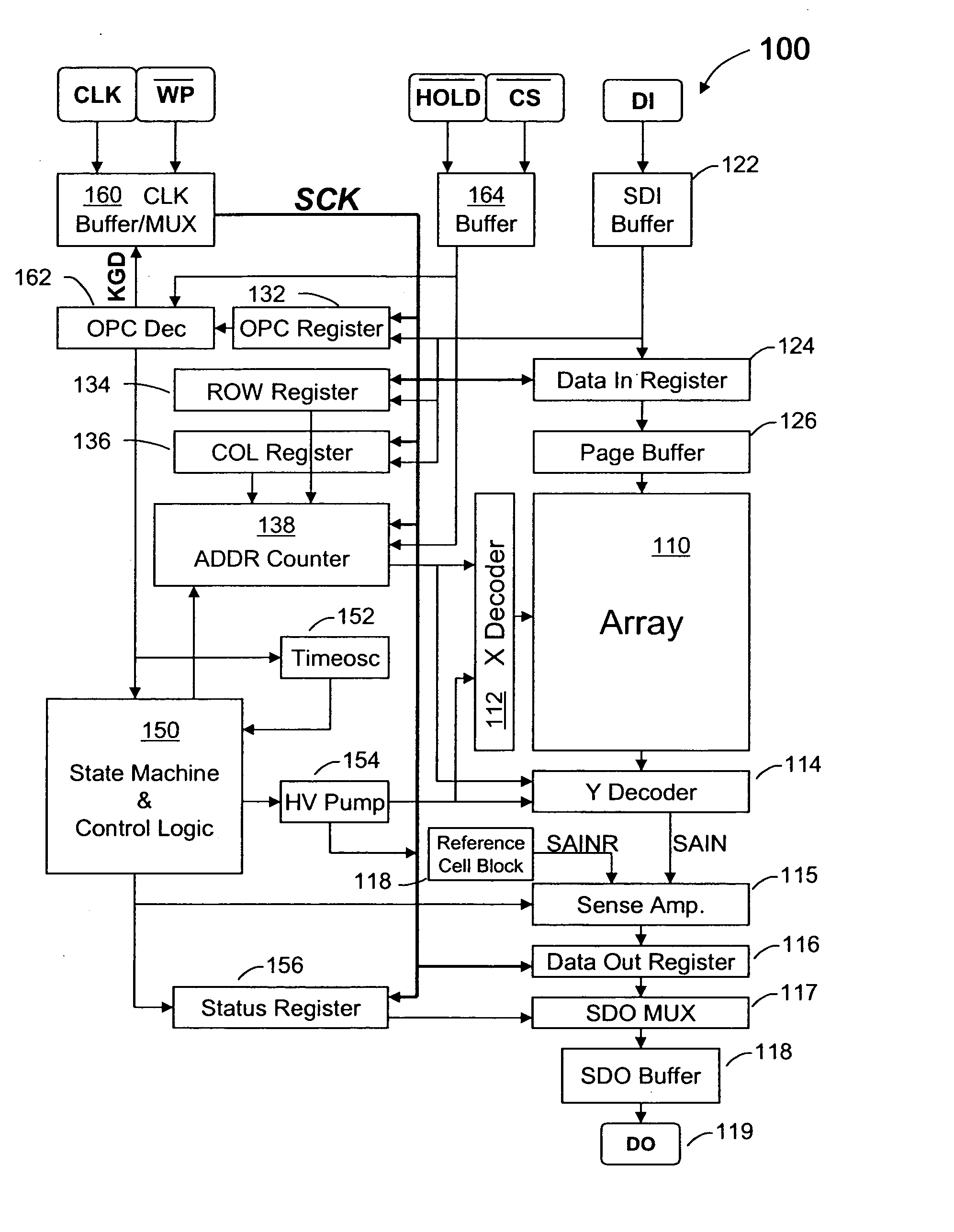
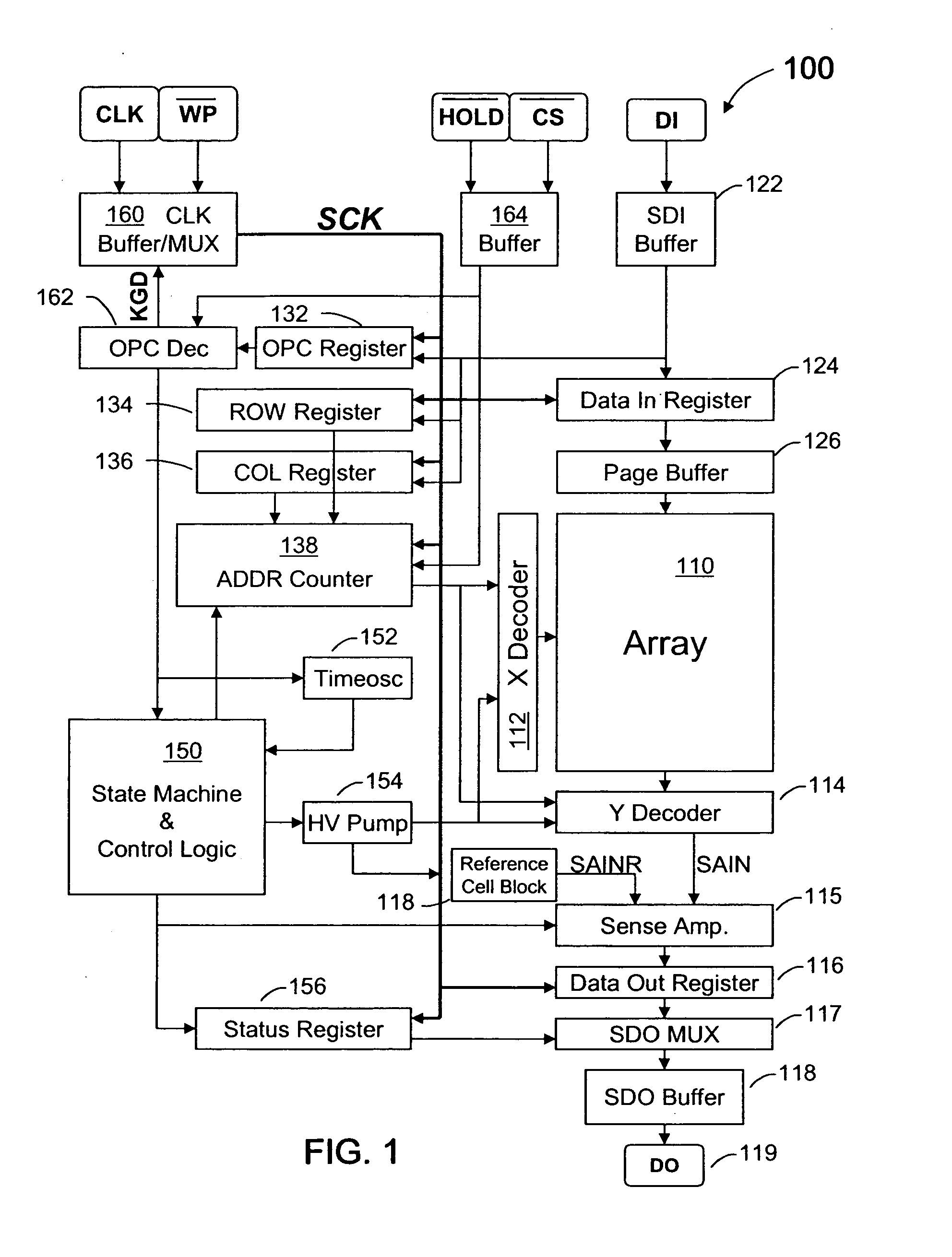
[0030]According to the present invention, techniques directed to integrated circuit memory testing and design are provided. More particularly, the invention provides a method and apparatus for memory device testing at a higher clock rate than the clock rate provided by a memory tester. Merely by way of example, the invention has been applied to serial flash memory devices for the manufacture of integrated circuits. But it would be recognized that the invention has a much broader range of applicability. For example, the invention can be applied to other memory devices such DRAM, SRAM, parallel flash, or other non-volatile memories The invention can also be applied to systems that include synchronized circuits.

[0031]Depending upon the embodiment, the present invention includes various features, which may be used. These features include the following:

[0032]1. Provide a method for testing a memory device at a high frequency using a low frequency tester;

[0033]2. Provide a design of a mem...


PUM


Abstract

Method and apparatus for memory device testing at a higher clock rate than the clock rate provided by a memory tester. The method includes providing a memory tester capable of generating a first clock signal characterized by a first clock frequency, and applying the first clock signal to the memory device. The method also includes receiving a command for activating a high-clock-frequency test mode. The method generates a second clock signal in the memory device in response to the first clock signal. The second clock signal is characterized by a second clock frequency which is higher than the first clock frequency. The method then tests the memory device at the second clock frequency. In a specific embodiment, the method is applied to a serial flash memory device. The invention can also be applied to testing and operating other memory devices or systems that include synchronized circuits.

Description

BACKGROUND OF THE INVENTION[0001]The present invention is directed to integrated circuits and their design for the manufacture of semiconductor devices. More particularly, this invention provides a method and apparatus for memory device testing at a higher clock rate than the clock rate provided by a memory tester. Merely by way of example, the invention has been applied to serial flash memory devices for the manufacture of integrated circuits. But it would be recognized that the invention has a much broader range of applicability. For example, the invention can be applied to other memory devices such DRAM, SRAM, parallel flash, or other non-volatile memories. The invention can also be applied to systems that include synchronized circuits.[0002]Flash memories are used in a variety of applications in electronics. These memories can retain data without the need for a power supply, and they are used for data and code storage in many applications, such as cell phones, digital cameras, p...

Claims


Application Information

Patent Timeline
IPC IPC(8): G11C16/06G11C29/00G11C7/00G11C11/34
CPCG11C7/22G11C29/14G11C29/12015G11C7/222
Inventor LIN, TIEN-LERKIM, KWANGHOCHEN, HUIPARK, EUNGJOON
Owner WINBOND ELECTRONICS CORP
Why Eureka
Try Eureka