SPI flash memory test system and method based on FT4222

A test system and test method technology, applied in the direction of static memory, instruments, etc., can solve the problems of frequent programming, inflexibility, trouble, etc., and achieve the effect of convenient modification and improved efficiency

Active Publication Date: 2018-01-26
NANJING HEYANGTEK CO LTD
View PDF11 Cites 8 Cited by
  • Summary
  • Abstract
  • Description
  • Claims
  • Application Information

AI Technical Summary

Problems solved by technology

This method has two disadvantages. One is that the bin file executed by the host is burned in the ROM, so during the test process, frequent burning is required, which is troublesome.
The second is that this kind of test can only test the function and response of SPI under normal conditions. In some special cases or the test content cannot be realized, it is not flexible enough.
At present, memory chips are widely used and in great demand. SPI NAND Flash is used in various devices, and the stability of Flash requires a large number of tests to ensure that the test of SPI NAND Flash requires a long time to read and write a large amount of data. Access and other complex operations, so a systematic method is needed to test Flash

Method used


Image

  • SPI flash memory test system and method based on FT4222

Examples


specific Embodiment approach

[0034] 1) First create a text document and input the commands to be tested. If there are multiple combinations, you need to input them on separate lines. The format is two-byte hexadecimal numbers separated by spaces, arranged in sequence, and press Enter after inputting. new line. Such as:

[0035] Write command 0x02+column addr+data

[0036] Read command 0x03 / 0x3b / 0x6b / 0xeb / 0xbb+column addr+length (two-byte hexadecimal)

[0037] 0x13 / 0x10+block / page addr

[0038] Erase command 0xd8+block addr

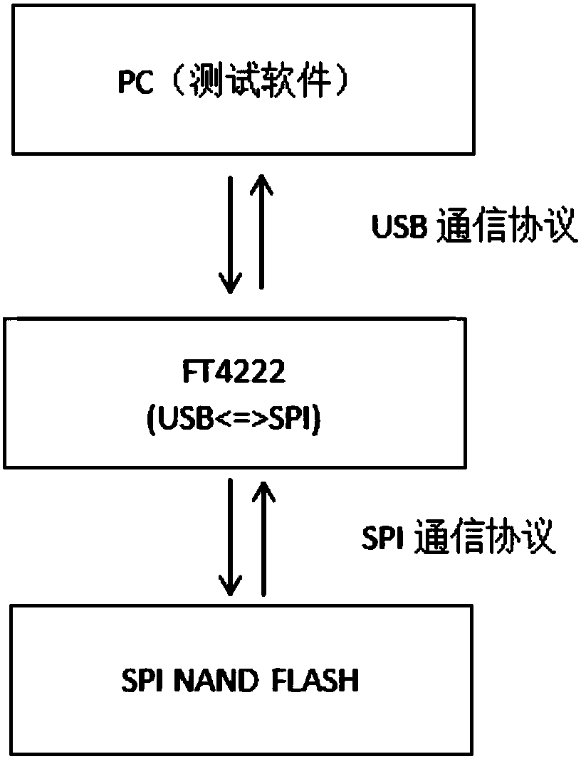
[0039] 2) After the script file is input, open the Debug Tool, click the Scan button, openFT4222device, and then set various flash parameters and test conditions on the interface, click the loadfile button after completion, load the command file just created, pass Programming calls the library function of FT4222 to realize the test work of SPI NAND Flash.

[0040] 3) The running result is displayed in the blank area on the right, and at the same time, the correctness of the comma...


PUM


Abstract

The invention discloses a SPI flash memory test system and a method based on FT4222. According to the SPI flash memory test method, calling of FT4222 chip equipment in a debugging tool is carried outbased on test statements input by testers, configuration of test conditions is carried out based on SPI NAND Flash modules of different parameters, and at last, loading of the test statements into theFT4222 chip modules is carried out so as to realize test of the SPI NAND Flash module. The method is capable of testing simple SPI NAND Flash reading, writing, and erasuring, and realizing BurnIn test (stability test), and achieving special test purposes via modifying test software program codes.

Description

technical field [0001] The invention relates to an FT4222-based SPI NAND Flash testing method, which belongs to the field of SPI NAND Flash testing. Background technique [0002] The SPI NAND Flash test is usually connected by two FPGA boards, one as the Host terminal and the other as the Device terminal. During the test, the Host terminal executes different instructions to test whether the various functions of the Device terminal are correct. This method has two disadvantages. One is that the bin file executed by the Host is burned in the ROM, so it needs to be burned frequently during the test process, which is troublesome. The second is that this kind of test can only test the function and response of SPI under normal conditions, and some special cases or test content cannot be realized, which is not flexible enough. [0003] Therefore, the FT4222 is used to simulate the behavior of the Host, and the instructions to be executed are edited in the text file. During the tes...

Claims


Application Information

Patent Timeline
Patent Type & Authority Applications(China)
IPC IPC(8): G11C29/56G11C29/04
CPCG11C29/04G11C29/56
Inventor 黄欢施冠良
Owner NANJING HEYANGTEK CO LTD
Why Eureka
Try Eureka