

Organic light emitting display device and method of fabricating the same
a light-emitting display and organic technology, applied in the direction of organic semiconductor devices, electroluminescent light sources, electric lighting sources, etc., can solve the problems of limited use of ag, single layer generally cannot be implemented, and ag, which has the highest reflectivity among metals, has been significantly limited in its use. , to achieve the effect of increasing the reflectivity and efficiency of organic light-emitting display devices, reducing the panel size of organic light-emitting display
Active Publication Date: 2009-03-31
SAMSUNG DISPLAY CO LTD
View PDF4 Cites 4 Cited by
- Summary
- Abstract
- Description
- Claims
- Application Information
AI Technical Summary
Benefits of technology
The present invention is about an organic light emitting display device and a method of fabricating it. The device uses an Ag alloy containing Sm, Tb, Au, and Cu to form the source and drain electrodes, as well as the first electrode. This results in increased reflectivity and efficiency of the device, as well as reduced panel size due to the low resistance of the source and drain electrodes. The method involves preparing a substrate, forming a thin film transistor, adding an organic layer with at least an organic emission layer, and adding a second electrode on top of the organic layer. The source, drain, and first electrodes are made of a reflective layer made of a silver (Ag) alloy with a specific composition ratio. The technical effects of this invention include increased reflectivity and efficiency of the organic light emitting display device, as well as reduced panel size.
Problems solved by technology
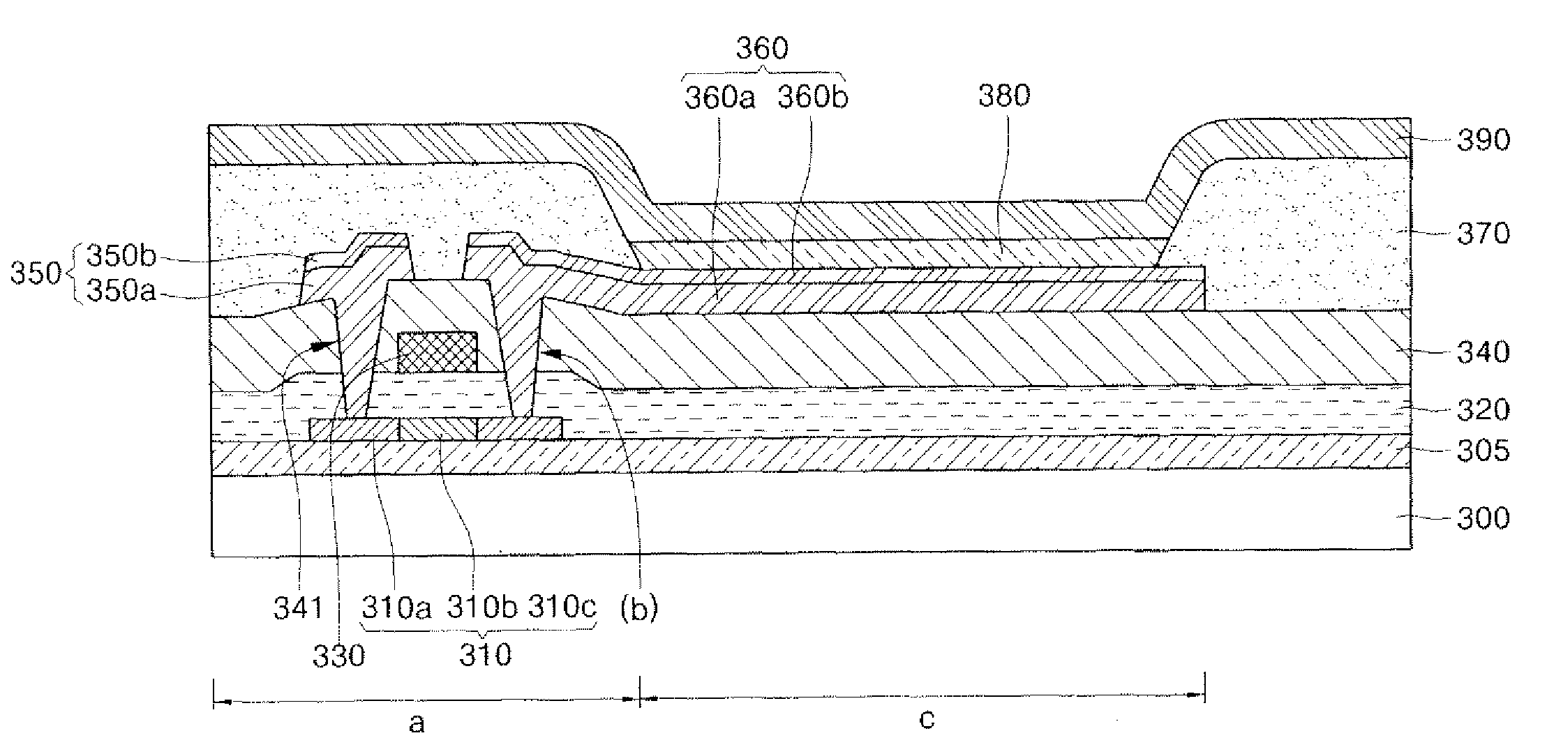
In the conventional active matrix organic light emitting display device of FIG. 1, Ag (1.61 μΩ-cm), used in the formation of the source electrode 150 and the drain electrode 155, is considered as an ideal, low-resistance interconnection material because of its low resistivity; however in manufacturing processes, the use of Ag has been limited because of Ag's weak adhesion, thermal instability, and poor chemical resistant property.
A single layer generally cannot be implemented because a step coverage or a hill-look problem causes a disconnection failure or affects a subsequent lithography process due to a change in reflectance.
When the conventional first electrode is formed as a reflective electrode, Ag, which has the highest reflectivity among metals, has been significantly limited in its use due to adhesion, thermal resistance, and chemical resistance.
To address Ag's material limitations, Al and an Al alloy were employed instead of Ag; however, use of Al or the Al alloy, caused the reflectivity and the efficiency to degrade.
Method used
View moreImage
Smart ImageViewing Examples

Examples
first embodiment
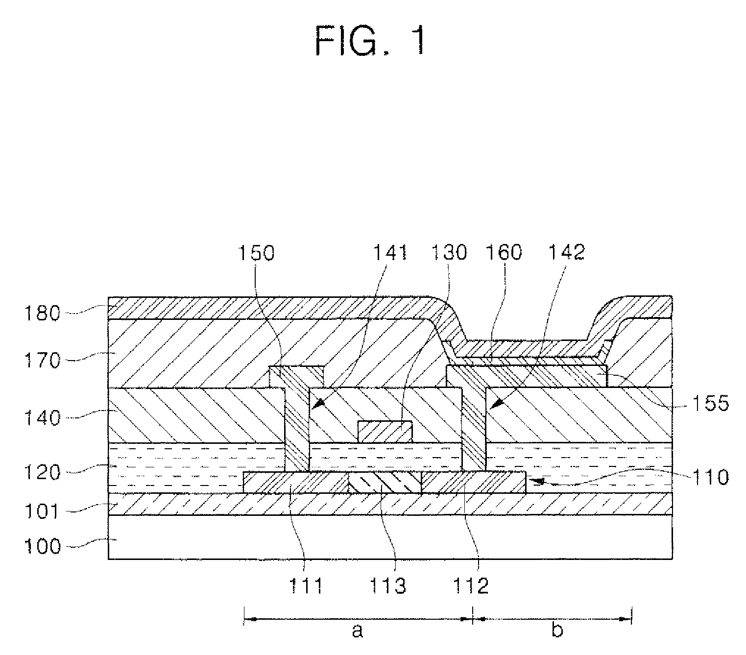
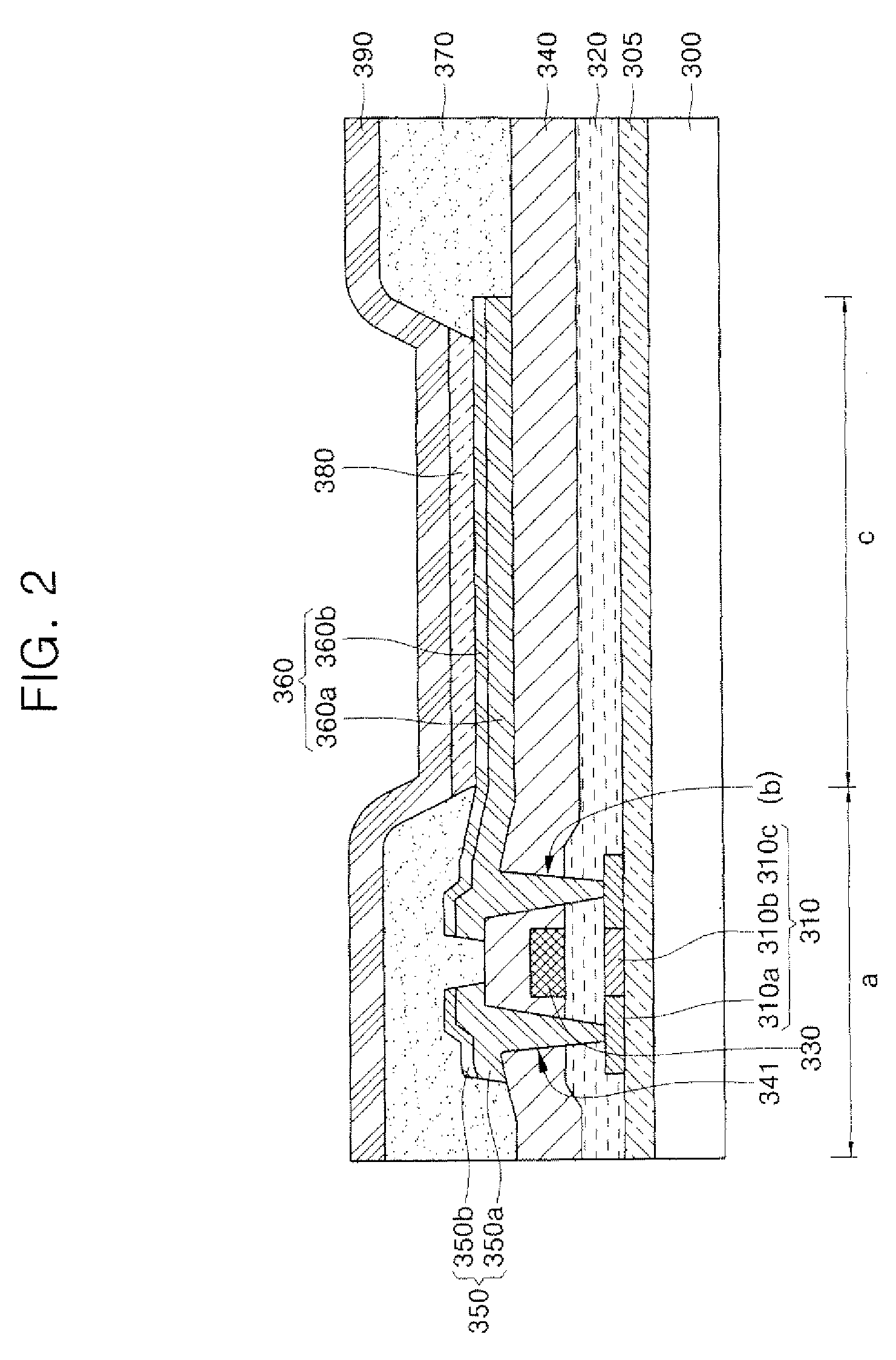
[0081]The source electrode 350 and the drain electrode 355 of the organic light emitting device were formed from an Ag alloy (a composition ratio of 0.3 atom % of Sm, 0.5 atom % of Tb, 0.4 atom % of Tb, and 0.4 to 1.0 atom % of Cu) having a thickness of 5000□ using a sputtering method. The remaining elements of the thin film transistor would have been identified as conventional elements for a thin film transistor to one of ordinary skill in the art.
Login to View More PUM
 Abstract
An organic light emitting display device and a method of fabricating the same are provided, which employ an Ag alloy containing Sm, Tb, Au, and Cu to simultaneously form a source electrode, a drain electrode, and a first electrode of the organic light emitting display device for increasing the reflectivity and efficiency of the organic light emitting display device and reducing the organic light emitting display device panel size by reducing a line width of the source and drain electrodes due to the low resistance of the source and drain electrodes.
Description
CROSS-REFERENCE TO RELATED APPLICATIONS[0001]This application claims priority to and benefit of Korean Patent Application No. 10-2005-0035729, filed Apr. 28, 2005, which is hereby incorporated by reference for all purposes as if fully set forth herein.BACKGROUND OF THE INVENTION[0002]1. Field of the Invention[0003]The present invention relates to an organic light emitting display device and a method of fabricating the same, and more particularly, to an organic light emitting display device including a first electrode, a source electrode, and a drain electrode simultaneously formed from a silver (Ag) alloy containing samarium (Sm), terbium (Tb), gold (Au), and copper (Cu), and a method of fabricating the same.[0004]2. Description of the Related Art[0005]The advantages of a conventional organic light emitting display device include: low power consumption, wide viewing angle, good contrast, and fast response speed.[0006]FIG. 1 is a cross-sectional view of a conventional top emission ac...
Claims
Login to View More Application Information
Patent Timeline
 Patent Type & AuthorityPatents(United States)
IPC IPC(8): H01L29/34
CPCH01L27/3244H01L27/3279H01L51/5218H01L2251/5315H01L2924/0002H01L2924/00H10K59/1315H10K2102/3026H10K59/80518H05B33/26H05B33/10H10K50/818H10K59/12
InventorSHIN, HYUN-EOK
OwnerSAMSUNG DISPLAY CO LTD