Ultra lightweight photovoltaic device and method for its manufacture

a photovoltaic device and lightweight technology, applied in the field of photovoltaic and other electronic devices, can solve the problems of difficult transportation of massive items, difficult to etch a substrate to a thickness of less than one mil, and difficult to manufacture photovoltaic devices

Inactive Publication Date: 2009-04-14
UNITED SOLAR OVONIC
View PDF9 Cites 27 Cited by
  • Summary
  • Abstract
  • Description
  • Claims
  • Application Information

AI Technical Summary

Problems solved by technology

The weight of photovoltaic devices is also of significant concern in other mobile applications, and in those particular applications in which transport of massive items is difficult.
However, it has been found that as a practical matter it is very difficult to etch a substrate down to a thickness of less than one mil.
A typical substrate material may include defects, contaminants, or regions of varying composition which result in non-uniform etching, and such features can cause the formation of pinholes, cracks, voids or the like in the etched substrate, and these defects can lead to delamination or other damage to adjacent portions of the electronically active material.
This difficulty in etching substrates has placed a limitation upon the fabrication of lightweight and ultra lightweight semiconductor devices.

Method used


Image

  • Ultra lightweight photovoltaic device and method for its manufacture
  • Ultra lightweight photovoltaic device and method for its manufacture

Examples


Embodiment Construction

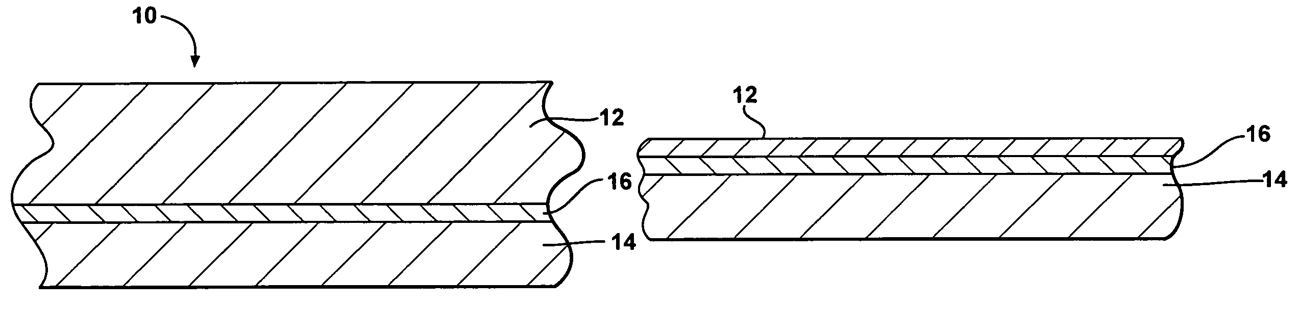
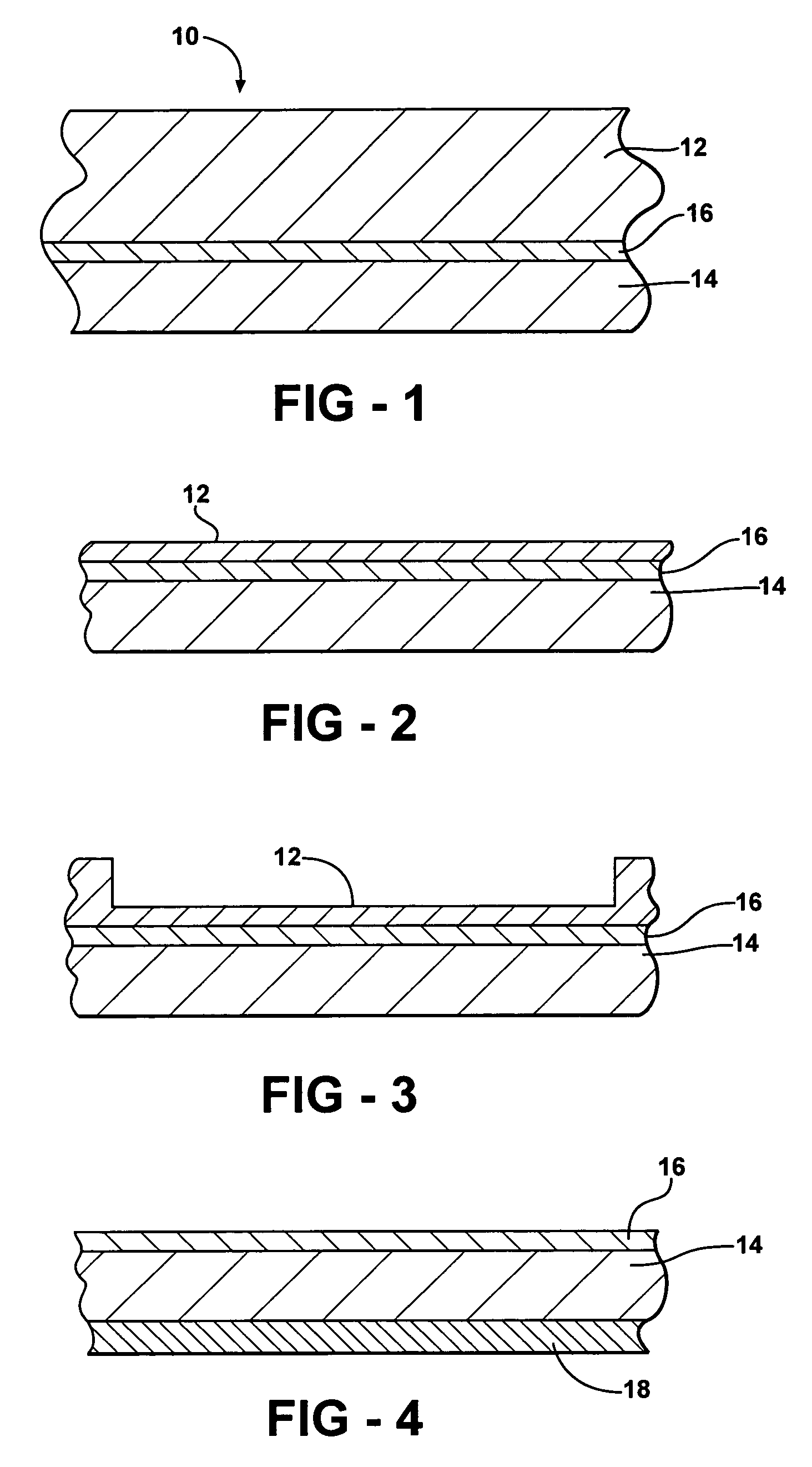
[0015]In accord with the present invention it has been found that an appropriate barrier layer of non-etchable material may be interposed between a substrate and a body of electronically active material. The barrier layer is very thin, but it is resistant to chemical etching. Accordingly, the barrier layer will allow for a substrate to be etched to a very small thickness, or even completely removed, without compromising the integrity of the remainder of the electronic device.

[0016]The present invention will be explained with reference to a photovoltaic device; however, it is to be understood that the principles of the present invention may be employed in connection with other types of electronic devices, particularly thin film semiconductor devices, including photoactive devices such as photosensors, photoconductors, light emitting devices and the like, as well as in conjunction with non-photoactive devices such as transistors, diodes, and integrated circuits.

[0017]Referring now to ...


PUM

PropertyMeasurementUnit
thicknessaaaaaaaaaa
thicknessesaaaaaaaaaa
thicknessaaaaaaaaaa

Abstract

An ultra lightweight semiconductor device such as a photovoltaic device is fabricated on a non-etchable barrier layer which is disposed upon an etchable substrate. The device is contacted with an appropriate etchant for a period of time sufficient to remove at least a portion of the thickness of the substrate. The barrier layer prevents damage to the photovoltaic material during the etching process. Photovoltaic devices fabricated by this method have specific power levels in excess of 300 w / kg.

Description

RELATED APPLICATION[0001]This application claims priority of U.S. Provisional Patent Application Ser. No. 60 / 620,808 filed Oct. 21, 2004, entitled “Ultra Lightweight Electronic Device and Method for its Manufacture” which is incorporated herein by reference.GOVERNMENT INTEREST[0002]This invention was made with Government support under contract F29601-03-C-0122 awarded by Air Force Research Laboratory. The United States Government has certain rights in the invention.FIELD OF THE INVENTION[0003]This invention relates generally to photovoltaic and other electronic devices. More particularly, the invention relates to ultra lightweight photovoltaic devices and methods for their fabrication.BACKGROUND OF THE INVENTION[0004]Weight is a very important factor in many electronic device applications. For example, photovoltaic generator arrays are frequently used as power sources in aerospace and military applications where weight is at a premium. The weight of photovoltaic devices is also of s...

Claims


Application Information

Patent Timeline
Patent Type & Authority Patents(United States)
IPC IPC(8): B29D11/00H01L31/06
CPCH01L31/0392H01L31/18Y02E10/50H01L31/042H01L31/0256
Inventor GUHA, SUBHENDUBANERJEE, ARINDAMBEERNINK, KEVINJOHNSON, TODDPIETKA, GINGERDEMAGGIO, GREGORYLIU, SHENGZHONG FRANKYANG, JEFFREY
Owner UNITED SOLAR OVONIC
Why Eureka
Try Eureka