Pixel structure and liquid crystal display panel
a liquid crystal display panel and pixel structure technology, applied in non-linear optics, instruments, optics, etc., can solve the problems that the cathode ray tube (crt) cannot meet the market demands gradually, and achieve the effect of increasing the aperture ratio enhancing the luminance of the lcd panel
- Summary
- Abstract
- Description
- Claims
- Application Information
AI Technical Summary
Benefits of technology
Problems solved by technology
Method used
Image
Examples
first embodiment
The First Embodiment
[0044]FIG. 2A is a partial schematic sectional view of an LCD panel according to the first embodiment of the present invention, and FIG. 2B is a top view of an active device array substrate according to the first embodiment of the present invention, wherein the schematic sectional view of the active device array substrate of FIG. 2A is taken along the section line B-B′ in FIG. 2B. Referring to FIGS. 2A and 2B, the LCD panel 600 of the present embodiment comprises a lower substrate 110, an upper substrate 140, a color filter array 150, and a plurality of pixel structures 200. A plurality of scan lines 120 and a plurality of data lines 130 are formed on the lower substrate 110. The color filter array 150 is disposed between the lower substrate 110 and the upper substrate 140. The pixel structures 200 are disposed between the color filter array 150 and the lower substrate 110. The detailed structure, arrangement position, connection relation, and material of various...
second embodiment
The Second Embodiment
[0056]FIG. 3A is a partial schematic sectional view of an LCD panel according to the second embodiment of the present invention, and FIG. 3B is a top view of an active device array substrate according to the second embodiment of the present invention, wherein the schematic sectional view of the active device array substrate of FIG. 3A is taken along the section line C-C′ in FIG. 3B. Referring to FIGS. 3A and 3B, the LCD panel 700 of the present embodiment is a variation of the LCD panel 600 of the first embodiment, and wherein the first pixel electrode 320 and the second pixel electrode 330 of the pixel structure 300 are respectively disposed on two opposite sides of the common line 270, and the coupling line 340 is not connected to the capacitor electrode 280.
[0057]As the advantages of the LCD panel 700 and the pixel structure 300 are substantially the same as those described in the first embodiment, the details will not be described herein again.
third embodiment
The Third Embodiment
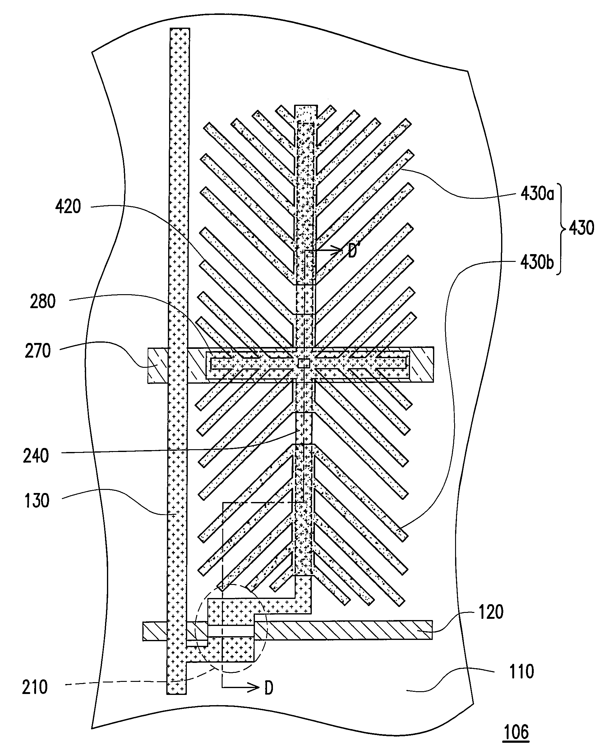
[0058]FIG. 4A is a partial schematic sectional view of an LCD panel 800 according to the third embodiment of the present invention, and FIG. 4B is a top view of an active device array substrate according to the third embodiment of the present invention, wherein the schematic sectional view of the active device array substrate of FIG. 4A is taken along the section line D-D′ in FIG. 4B. Referring to FIGS. 4A and 4B, the LCD panel 800 of the present embodiment is a variation of the LCD panel 600 of the first embodiment, and wherein the second pixel electrode 430 of the pixel structure 400 comprises a first sub-pixel electrode 430a and a second sub-pixel electrode 430b. And the first sub-pixel electrode 430a and the second sub-pixel electrode 430b are disposed respectively on two opposite sides of the first pixel electrode 420.
[0059]As the advantages of the LCD panel 800 and the pixel structure 400 are substantially the same as those described in the first embodiment...
PUM
| Property | Measurement | Unit |
|---|---|---|
| pixel structure | aaaaa | aaaaa |
| luminance | aaaaa | aaaaa |
| angle | aaaaa | aaaaa |
Abstract
Description
Claims
Application Information


