

Method of monitoring an erase threshold voltage distribution in a NAND flash memory device
a technology of erase threshold and nand flash memory, which is applied in the direction of digital storage, static storage, instruments, etc., can solve the problems of difficult to verify whether or not the erase threshold voltage distribution is improved, difficult to measure a negative threshold voltage value, and difficult to verify the erase threshold voltage distribution. to achieve the effect of accurate measuremen
- Summary
- Abstract
- Description
- Claims
- Application Information
AI Technical Summary
Benefits of technology
Problems solved by technology
Method used
Image


Examples
Embodiment Construction
[0026]Hereinafter, the preferred embodiments of the present invention will be explained in more detail with reference to the accompanying drawings.
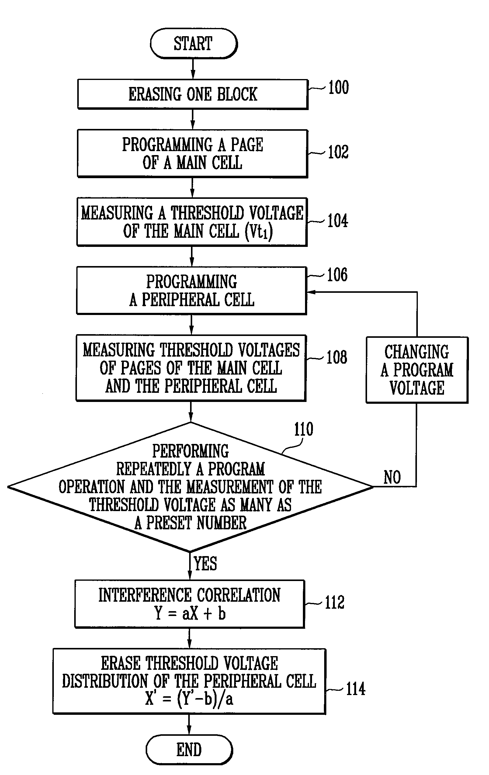
[0027]FIG. 1 is a flowchart illustrating a method of monitoring an erase threshold voltage distribution in a NAND flash memory device according to one example embodiment of the present invention.
[0028]In FIG. 1, a memory block is erased by applying an erase voltage to the memory block in step S100.
[0029]In step S102, a program operation is performed by applying a first program voltage Vpgm1 to a main cell for measuring an erase threshold voltage.
[0030]In step S104, a program threshold voltage Vt1 of the main cell is measured after the program operation is performed.
[0031]In step S106, a program operation of a peripheral cell is performed by applying a second program voltage Vpgm2 to the peripheral cell. Here, the peripheral cell is a cell next to the main cell, e.g. in a direction of a bit line or in a direction of a word line.
[0032]In st...
PUM
 Abstract
Description
Claims
Application Information