Volume based extended defect sizing system

a defect sizing and volume-based technology, applied in the direction of mechanical measurement arrangement, instruments, nuclear elements, etc., can solve the problems of high scattering power of a detected defect, measurement becomes nonlinear, and data extrapolation techniques are often difficult to perform in conventional wafer inspection systems

Active Publication Date: 2009-05-26
KLA TENCOR TECH CORP
View PDF7 Cites 7 Cited by
  • Summary
  • Abstract
  • Description
  • Claims
  • Application Information

AI Technical Summary

Benefits of technology

[0015]A threshold detection intensity may be used to qualify the intensity response shape volume, such as by forming the response volume mapping with scatter light intensity values that are above a given threshold. For example, the threshold may be used to help eliminate low level “haze” or noise that might cause spurious scatter light intensity readings.

Problems solved by technology

Such localized light scatters may be indicative of one or more defects on the wafer surface that may render an integrated circuit(s) (IC) fabricated on the wafer to be inoperative.
One drawback of the above-described conventional laser-based surface scanning inspection system is that the maximum scattering power of a detected defect may exceed the dynamic range of the system.
As a result, the electronics within the wafer inspection system may saturate, thereby causing at least some of the defect size measurements performed by the system to be at a power level at which the measurements become nonlinear due to the saturation effects.
However, such data extrapolation techniques are often difficult to perform in conventional wafer inspection systems.
However, conventional algorithms for performing such nonlinear least squares fit techniques often require a significant amount of processing time.
Further, relatively small changes in the data resulting from, e.g., noise or a non-ideal signal, may lead to significantly large changes in the estimated parameters.
There is a drawback to the methodology in that it adds some difficulty because it uses a completely separate calibration process, which can be time consuming and cumbersome.
This methodology has the drawback of requiring an unclipped or unsaturated signal level.
If the signal is clipped, correction of areas for filter effects is imperfect and performance may be degraded.
This methodology is also limited in range over which extrapolation is useful, as well as being computationally intensive.
However, this technique also uses an unclipped signal and can be extremely sensitive to variations from an ideal Gaussian response.

Method used


Image

  • Volume based extended defect sizing system
  • Volume based extended defect sizing system
  • Volume based extended defect sizing system

Examples


Embodiment Construction

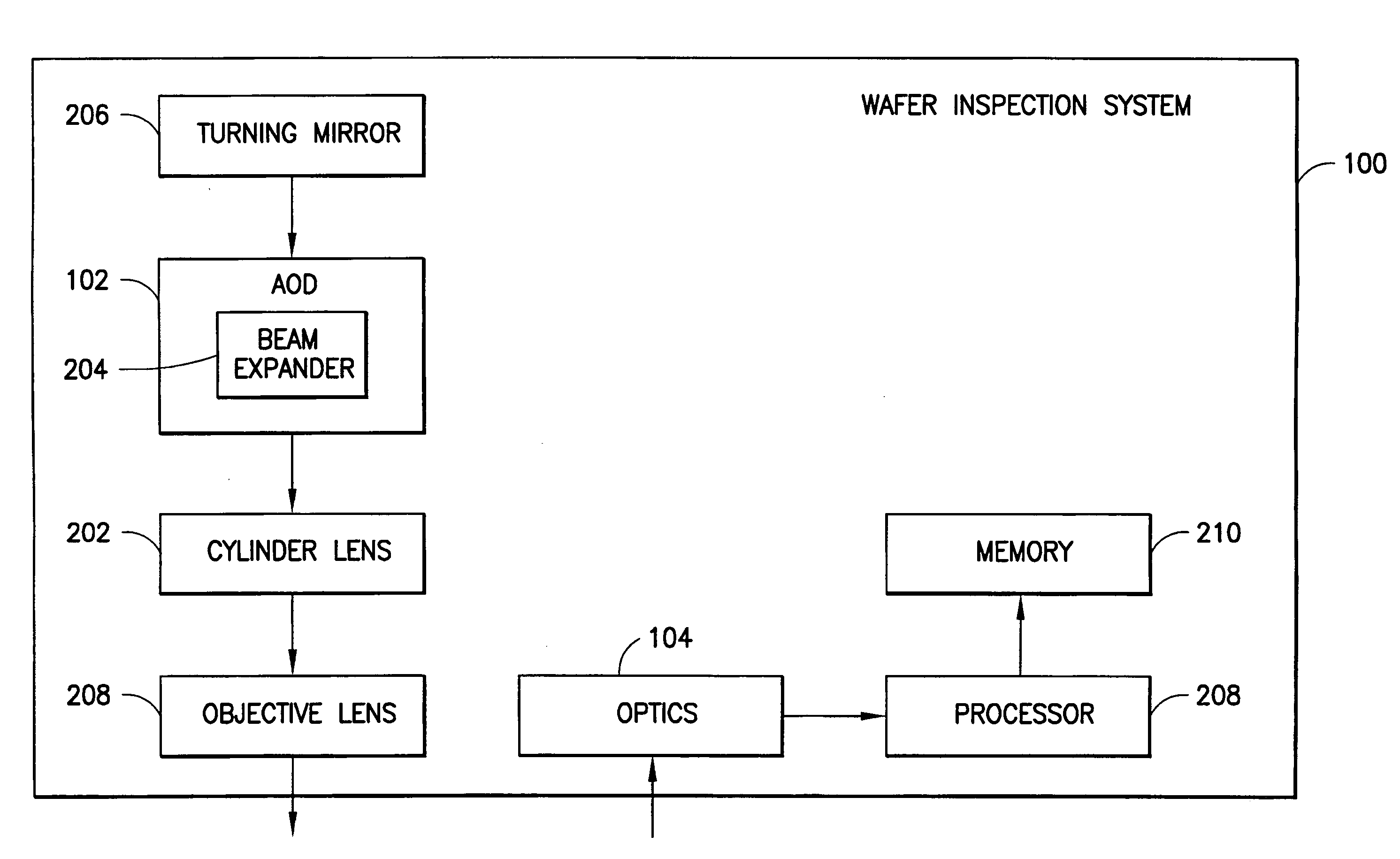
[0039]A system and method of inspecting a semiconductor wafer is disclosed that is capable of measuring the size and determining the location of a defect on a surface of a semiconductor wafer. The presently disclosed wafer inspection system can perform such sizing and locating of wafer surface defects whether or not the scattering power associated with the defect exceeds the dynamic range of the system.

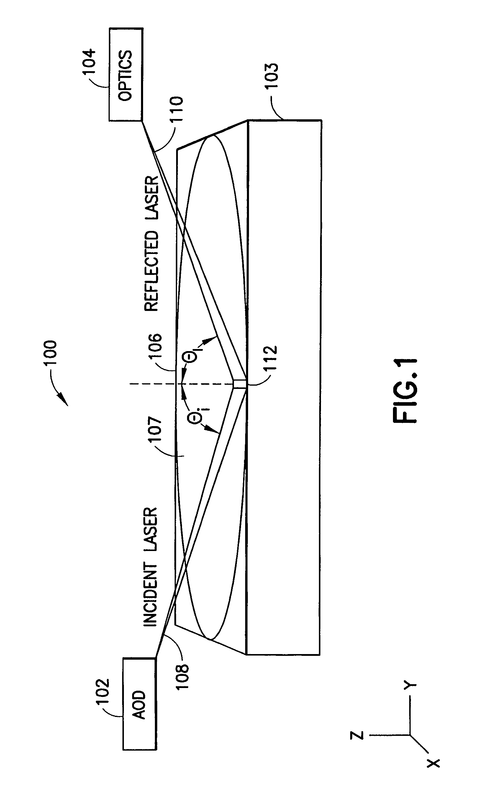
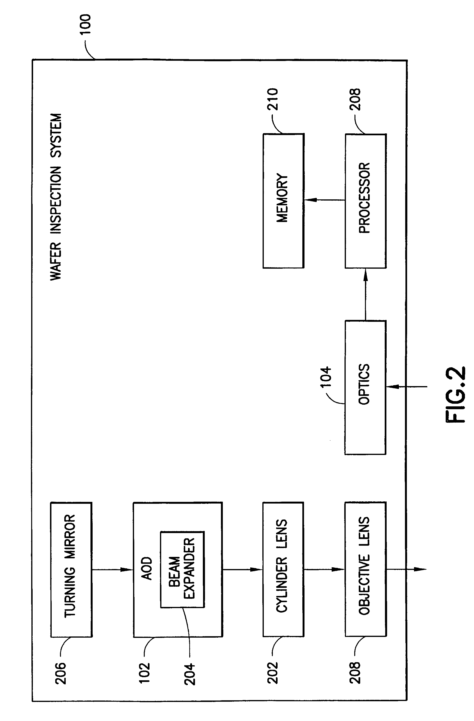
[0040]FIG. 1 depicts an illustrative embodiment of a laser-based wafer surface scanning inspection system 100, in accordance with the present invention. In the illustrated embodiment, the surface scanning inspection system 100 comprises an optical module including a surface scanning mechanism 102, and optics 104. Optics 104 include a light detector with a channel for detecting reflected light, often referred to as a “light channel”. A light detector with a channel for detecting scattered light, often referred to as a “dark channel” is also included in optics 104. For example, the surf...


PUM


Abstract

A system and method for sizing semiconductor wafer defects combines contiguous light intensity values over a defect area of the wafer to provide a defect sizing metric. The light intensity values resulting from a light source applied to the wafer are summed and the summation is compared to known metric values related to known defect sizes. The result of the comparison provides an estimate for the defect size under consideration. The combination of the light intensity values produces defect sizing estimates in saturated and unsaturated ranges of operation for the wafer inspection equipment. Calculations applied to the combined light intensity values vary depending upon whether the light intensity component is from a saturated or an unsaturated measurement. The defect sizing metric can be applied continuously in saturated and unsaturated ranges of operation to avoid additional processing steps, such as recalibration of the inspection equipment.

Description

CROSS REFERENCE TO RELATED APPLICATIONS[0001]This application is a continuation-in-part application of U.S. patent application Ser. No. 11 / 321,689 filed Dec. 29, 2005 now U.S. Pat. No. 7,302,360 entitled DEFECT SIZE PROJECTION, which is a continuation-in-part application, of U.S. patent application Ser. No. 10 / 971,694 filed Oct. 22, 2004, now U.S. Pat. No. 7,184,928 entitled EXTENDED DEFECT SIZING, which claims benefit of U.S. Provisional Patent Application No. 60 / 514,289 filed Oct. 24, 2003 entitled EXTENDED DEFECT SIZING.STATEMENT REGARDING FEDERALLY SPONSORED RESEARCH OR DEVELOPMENT[0002]Not applicableBACKGROUND OF THE INVENTION[0003]1. Field of Invention[0004]The present invention relates generally to systems and methods of inspecting semiconductor wafers, and relates more specifically to a semiconductor wafer inspection system, and method capable of detecting and measuring wafer defect's in which the scattering power of the defect exceeds the dynamic range of the system.[0005]2...

Claims


Application Information

Patent Timeline
Patent Type & Authority Patents(United States)
IPC IPC(8): G06F3/00
CPCG01N21/9501H01L21/67288
Inventor BELL, ERNESTJUDELL, NEIL
Owner KLA TENCOR TECH CORP
Why Eureka
Try Eureka