Variably responsive photosensor

a photosensor and variable technology, applied in the field of photosensors, can solve the problems of photon shot noise and read noise, source of noise in the photosensor array, and photon shot noise, and achieve the effect of increasing the signal generated in the photosensor

Active Publication Date: 2009-06-30
STMICROELECTRONICS (RES & DEV) LTD
View PDF8 Cites 8 Cited by
  • Summary
  • Abstract
  • Description
  • Claims
  • Application Information

AI Technical Summary

Benefits of technology

[0032]For purposes of discussion, the photosensor will be referred to a variable response photosensor. The variable response photosensor may comprise at least one switchable photosensitive site per photosensor. This allows a single photosensor to operate under either high light levels (with low photon-shot noise) or low light levels (with low readout-noise).
[0034]The variable response photosensor may connect unused photosensitive regions to a lower potential (e.g., ground). This causes photogenerated electrons to be preferentially drawn to the positively charged collection node. In effect, this causes the reduction in collection area (resulting from the use of a smaller number of photosensitive regions) to be less than the coinciding reduction in photosensor capacitance.
[0035]In general, the variable response photosensor may increase the signal generated in a photosensor by a factor of M. In other words, the variable response photosensor may enable the SNR of the photosensor to increase by M.

Problems solved by technology

There are two main sources of noise in a photosensor array, namely photon shot noise and read noise.
Photon shot noise results from natural fluctuations in the number of photons detected by a photosensor, and is caused by the quantum statistical nature of photon emission and detection.
Thus, photon shot noise imposes a fundamental limit on the responsivity of a photosensor array insofar as it determines the minimum noise level achievable therein.
However, as will be recalled, the full well capacity of a photosensor array provides an upper limit on the number of photons that can be integrated in its photosensors.
However, having a large full well capacity can present problems at low light levels.
Unfortunately, one of the major components of read noise is reset noise, which depends on the capacitance of the photosensor.
Accordingly, any attempt to reduce the read noise of a photosensor (by reducing its full well capacity) conflicts with increasing dynamic range and reducing photon shot noise.
However, the photosensing device in U.S. Pat. No. 5,296,698 is a lateral device, which is not suitable for use in photosensor arrays.
While this approach works well for small (<5 μm) photosensors, it is not as effective for larger (≧30 μm) photosensors.
Under these conditions, the dominant source of noise in the photosensor array is read noise.
Photosensors with a low capacitance typically have high sensitivity but increased photon shot noise.
In contrast, photosensors with a high capacitance typically have low photon shot noise but low sensitivity.
However, the lower sensitivity of such photosensors means that read noise provides a more significant contribution to the overall noise of the photosensor.
Consequently, the relative noise level of the photosensor is increased.

Method used


Image

  • Variably responsive photosensor
  • Variably responsive photosensor
  • Variably responsive photosensor

Examples


second embodiment

[0046]TABLE 1 lists the operating parameters of the variable response photosensor of FIGS. 9 and 10.

[0047]

TABLE 1LightActiveLevelCapacitanceSensitivityRegionsHL1LH1HL2LH2HL3LH3HighHighLow1, 2, 3, 4101010MediumMediumMedium1, 3, 4011010HighHighLowMediumMediumMedium1, 4010110LowLowHighLowLowHigh1010101

[0048]The following description will provide a brief overview of the concept underlying the variable response photosensor. This will be followed by a more detailed explanation of a first embodiment of the variable response photosensor comprising only two photosensitive regions. In particular, the discussion will focus on the structure of the first embodiment of the variable response photosensor and its operation with reference to the electric fields developed therein. The detailed description will finish with a description of a second embodiment of the variable response photosensor comprising multiple photosensitive regions.

[0049]The following descriptions are based on an embodiment compr...

first embodiment

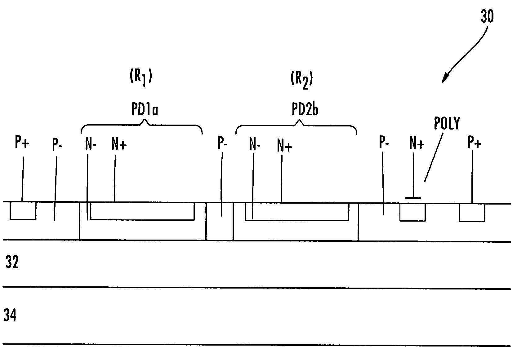
[0063]the variable response photosensor comprising two photosensitive regions will now be discussed. In terms of structural aspects, the isolation, at low light levels, of the diode and capacitance of the second photosensitive region (i.e., Dp2 / Cpd2) from the sense node (M1) by the transistor M6 is best explained by examining an exemplary pixel employing the variable response photosensor in FIG. 4 whose internal semiconductor structure is shown in FIG. 5. It will be noted that the position and size of transistors M1 to M6 depicted in FIG. 4 are provided for illustration purposes only. In particular, the actual size and layout of the transistors may be altered to satisfy individual system performance requirements (e.g., pixel size, noise, speed, power consumption, etc.).

[0064]Referring to FIG. 4, let a pixel 30 comprise a first variable response photosensor (PD1) and a second variable response photosensor (PD2). Let the first variable response photosensor (PD1) be divided into two ph...


PUM

PropertyMeasurementUnit
photosensitiveaaaaaaaaaa
voltageaaaaaaaaaa
exposure timeaaaaaaaaaa

Abstract

A photosensor includes a plurality of photosensitive regions including a first photosensitive region connected to a first voltage reference, and at least one additional photosensitive region. A signal collector is connected to the first photosensitive region. At least one switching device is for switching the at least one additional photosensitive region between the first voltage reference and a second voltage reference that is less than the first voltage reference, and for reversibly connecting the at least one additional photosensitive region to the signal collector so that the photosensor is variably responsive to different light levels.

Description

FIELD OF THE INVENTION[0001]The present invention relates to photosensors, and more particularly, to a photosensor in which its response may be varied in accordance with different lighting conditions.BACKGROUND OF THE INVENTION[0002]It is often desirable for a photosensor array to contain at least one photosensor capable of operating under a variety of different lighting conditions (e.g., high light levels) and poorly lit conditions (e.g., low light levels). This feature is typically provided by changing the exposure time of the photosensor. For example, under bright lighting conditions, the exposure time of the photosensor is reduced to prevent the photosensor from saturating.[0003]Since the present invention relates to the response of a photosensor under different lighting conditions, it is useful at this point to briefly review a number of the operating characteristics of photosensors in reference to FIGS. 1 and 2.[0004]The full well capacity of a photosensor array refers to the ...

Claims


Application Information

Patent Timeline
Patent Type & Authority Patents(United States)
IPC IPC(8): H01L31/00H01L27/15H01L29/16H01L29/161H01L29/26H01L29/417H01L29/74H01L31/109H01L31/111H01L31/12H01L31/153H01L33/00
CPCH04N3/155H04N5/3559H04N5/37452H04N25/59H04N25/771
Inventor RAYNOR, JEFFREY
Owner STMICROELECTRONICS (RES & DEV) LTD
Why Eureka
Try Eureka