Back-illuminated global pixel unit structure and preparation method thereof

A pixel unit and back-illuminated technology, which is applied in the field of back-illuminated global pixel unit structure and its preparation, can solve the problems of storage capacitor area limitation, reduce the sensitivity of pixel unit, reduce the photosensitive area of ​​photodiode, etc., and achieve the reduction of readout Effects of noise, distortion prevention, and increased capacitance

Active Publication Date: 2020-06-09
SHANGHAI INTEGRATED CIRCUIT RES & DEV CENT +1
View PDF8 Cites 0 Cited by
  • Summary
  • Abstract
  • Description
  • Claims
  • Application Information

AI Technical Summary

Problems solved by technology

[0011] At the same time, the capacitance values ​​of storage capacitors C1 and C2 also directly affect the readout noise of the global pixel unit. The larger the capacitance value of storage capacitors C1 and C2, the smaller the readout noise of the pixel unit and the better its performance. Conventional storage capacitors C1 and C2 use MOS capacitors, and the capacitance value is proportional to its area, but if the area of ​​the storage capacitor is increased, the photosensitive area of ​​the photodiode needs to be reduced, which will reduce the sensitivity of the pixel unit. Therefore, in order to ensure that the photodiode in the pixel unit area of ​​the photosensitive area, the area of ​​the storage capacitor is limited

Method used


Image

  • Back-illuminated global pixel unit structure and preparation method thereof
  • Back-illuminated global pixel unit structure and preparation method thereof
  • Back-illuminated global pixel unit structure and preparation method thereof

Examples


Embodiment Construction

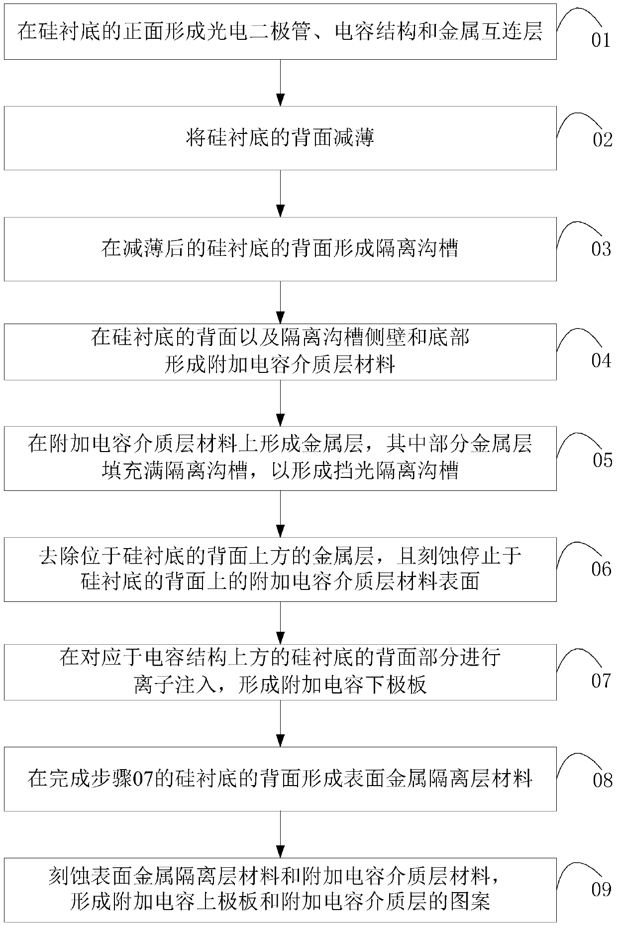
[0040] In order to make the content of the present invention clearer and easier to understand, the content of the present invention will be further described below in conjunction with the accompanying drawings. Of course, the present invention is not limited to this specific embodiment, and general replacements known to those skilled in the art are also covered within the protection scope of the present invention.

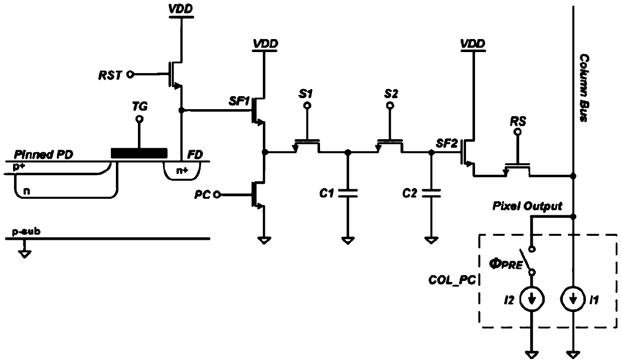
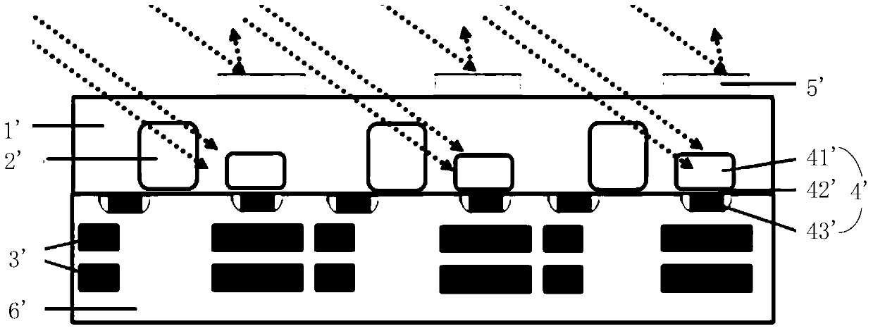
[0041] The back-illuminated global exposure pixel unit structure of the present invention can prevent light leakage and increase the capacitance value of the storage capacitor to prevent the impact of incident light on the charge signal escaped from the capacitor, avoid distortion of the output signal, and increase the capacitance in the global pixel unit. The capacitor value can improve the signal-to-noise ratio and finally get a high-quality image. The back-illuminated global pixel unit structure of the present invention can be applied to CMOS image sensors, and ...


PUM

PropertyMeasurementUnit
thicknessaaaaaaaaaa

Abstract

The invention provides a backside illumination global pixel unit structure and a preparation method thereof. The preparation method includes the following steps: conducting reflection of incident light by using a light-blocking isolation groove and an additional capacitance top crown, preventing the incident light from entering a charge signal memory block of a capacitor structure, and forming an additional capacitor structure on a back surface of a silicon lining in correspondence to the capacitor structure, the additional capacitor structure being in parallel to the capacitor structure. The backside illumination global pixel unit structure does not take too much an area of a pixel unit, does not influence a photosensitive area of a photodiode in the pixel unit, does not low agility of a device, can increase memory capacitance of the global pixel unit, lowers readout noise of the global pixel unit and increases entire performance of the global pixel unit.

Description

technical field [0001] The invention relates to the technical field of semiconductors, in particular to a back-illuminated global pixel unit structure and a preparation method thereof. Background technique [0002] An image sensor refers to a device that converts optical signals into electrical signals. Generally, large-scale commercial image sensor chips include charge-coupled device (CCD) and complementary metal-oxide semiconductor (CMOS) image sensor chips. [0003] Compared with traditional CCD sensors, CMOS image sensors have the characteristics of low power consumption, low cost and compatibility with CMOS technology, so they are more and more widely used. CMOS image sensors are now not only used in consumer electronics, such as miniature digital cameras (DSC), mobile phone cameras, video cameras and digital single-lens reflex (DSLR), but also in automotive electronics, monitoring, biotechnology and medical fields. . [0004] The pixel unit of the CMOS image sensor i...

Claims


Application Information

Patent Timeline
Patent Type & Authority Patents(China)
IPC IPC(8): H01L27/146
CPCH01L27/1463H01L27/1464H01L27/14689
Inventor 顾学强赵宇航周伟
Owner SHANGHAI INTEGRATED CIRCUIT RES & DEV CENT
Why Eureka
Try Eureka