
PCB connector with identifiable characters

a connector and identifiable technology, applied in the field of connectors, can solve the problems of confusion and uncertainty, user may get confused quite easily, and all types of connectors may still be troublesome, and achieve the effects of avoiding misinsertion, saving assembly time of a computer, and being easy to recogniz

Active Publication Date: 2009-07-14
GIGA BYTE TECH CO LTD
View PDF5 Cites 18 Cited by
  • Summary
  • Abstract
  • Description
  • Claims
  • Application Information

AI Technical Summary

Benefits of technology

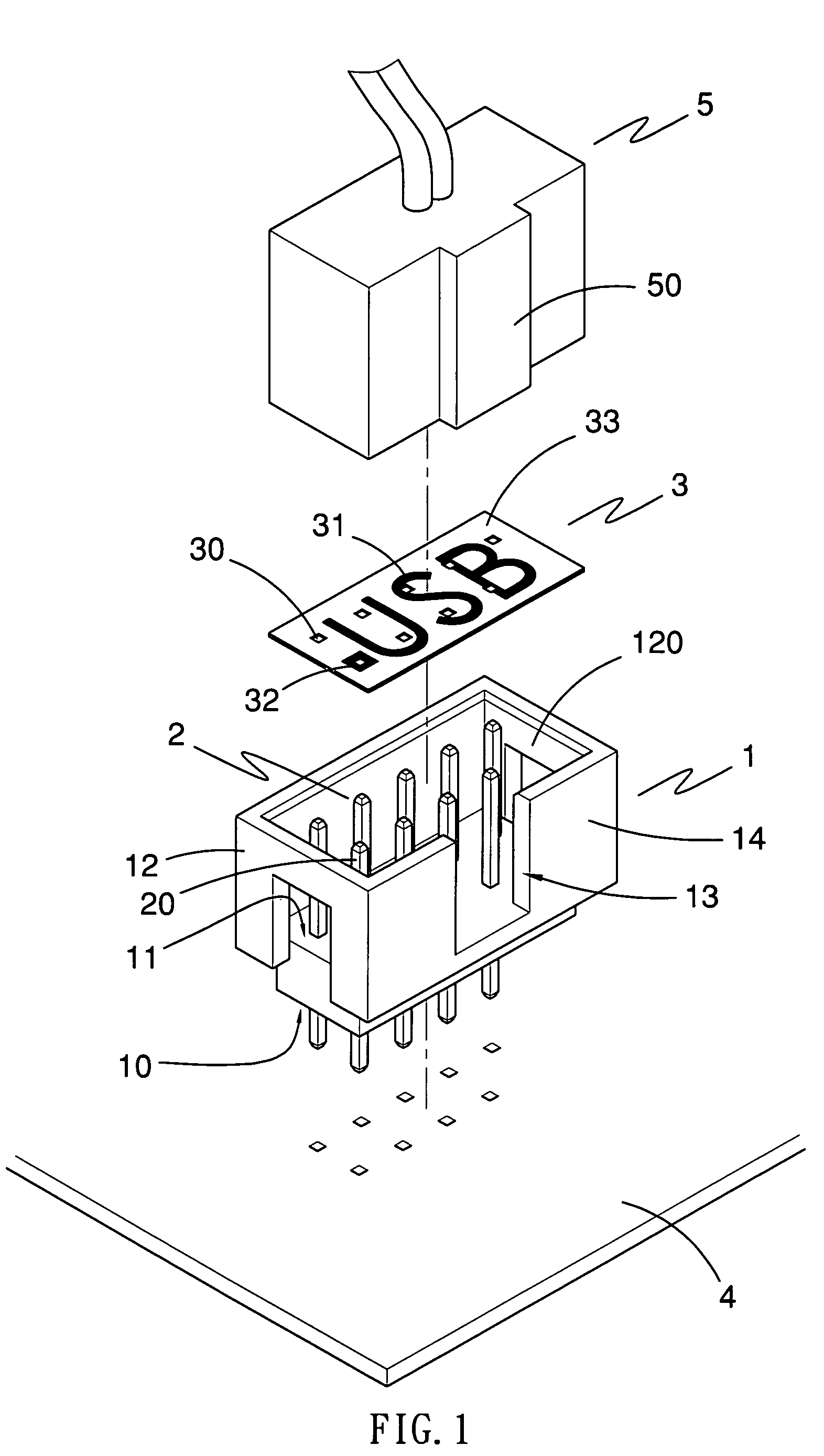
[0005]Broadly stated, the present invention is directed to a PCB connector or connector socket for connection to a printed circuit board. The PCB connector includes a body, a plurality of contact pins on both side of the body, and an identification layer joined to one side of the body. In particular, the identification layer defines a plurality of holes for insertion of the contact pins. The identification layer includes at least one character thereon for identifying function or use of the connector and a background in a color different from that of the character. Due to the distinct character(s) of the identification layer, the PCB connector is easily recognized, and therefore the assembly time of a computer is greatly saved and misinsertion is prevented.

Problems solved by technology

However, there are still a number of things about installing or building up a computer which causes confusion and uncertainty to those who are new to this activity.
For example, in a case where connectors are so similar to one another, except the number of the contact pins, a user may get confused quite easily due to inattention even if a Computer's User Manual for information is at hand.
Without distinct identification, all types of connectors may still be troublesome to be distinguished from one another and be inserted by a suitable external connector plug or device, (particularly if the person performing the installation hasn't had much practice).
It may take long time merely to correctly assemble a computer and ensure its correct functionality and long life.

Method used


Image

  • PCB connector with identifiable characters
  • PCB connector with identifiable characters
  • PCB connector with identifiable characters

Examples


Embodiment Construction

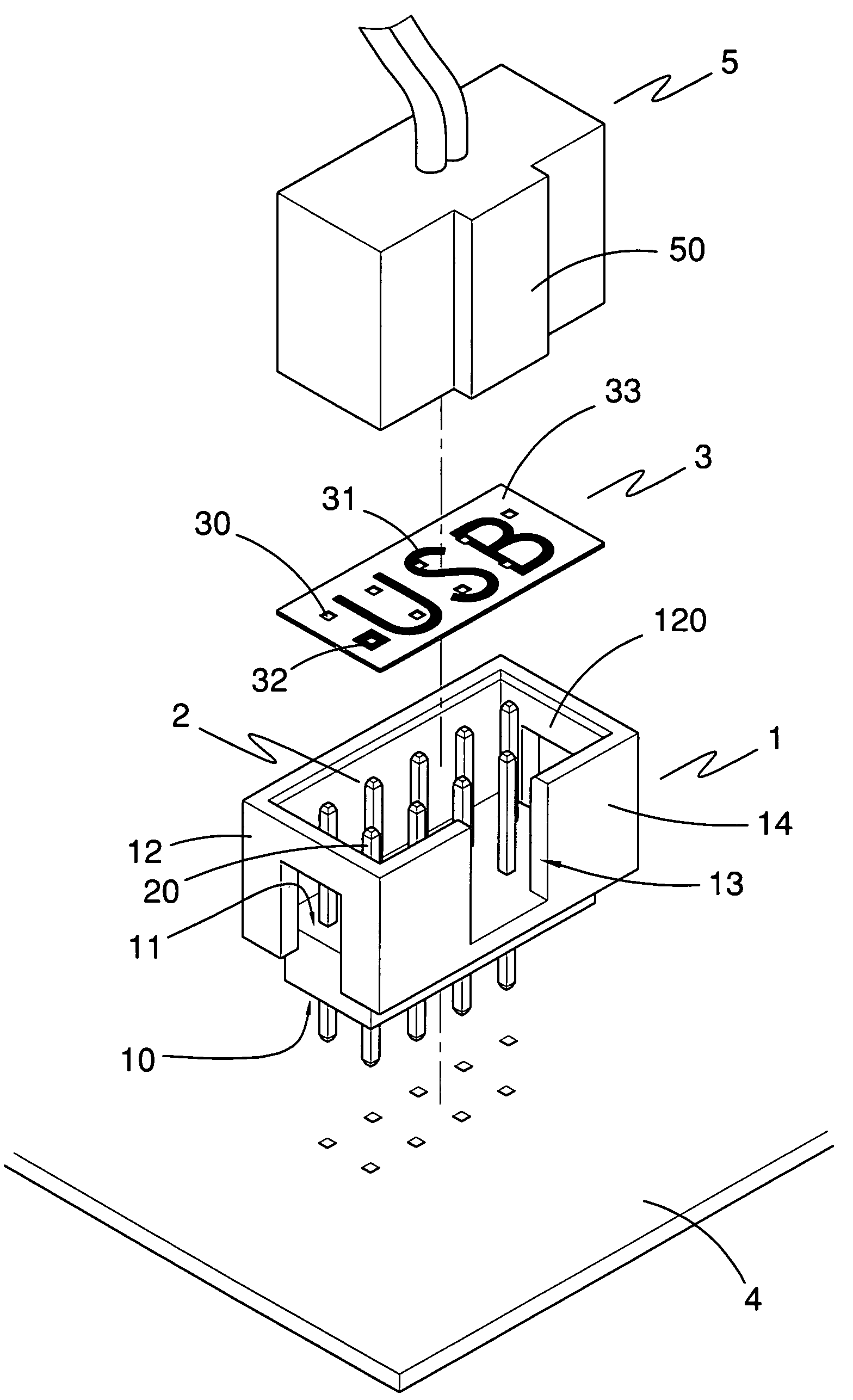
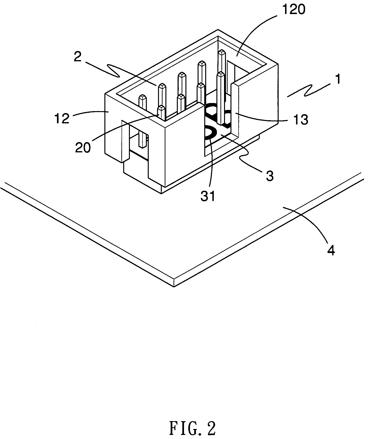
[0015]Referring now to FIGS. 1-3, a PCB connector or a connector socket according to the present invention is mounted on a printed circuit board 4 and includes a body 1, a plurality of contact pins 2 and an identification layer 3. Referring to FIGS. 1 and 2, the body 1 has a first surface 10 and a second surface 11 opposite the first surface 10. The first surface 10 faces the printed circuit board 4. The body 1 is formed with a peripheral frame 12 extending upward around the second surface 11. The peripheral frame 12 and the second surface 11 together define a receptacle 120 for receiving an external connector 5 or an external device. A fool-proof notch 13 is defined in a side wall 14 of the peripheral frame 12 and is dimensioned to conform to a protrusion 50 of the external connector 5 to ensure that a wrong type of device is not inserted. In such a fashion, the PCB connector is protected from misalignment of the external connector 5 or misinsertion of a wrong type of external conn...


PUM


Abstract

A connector for connection to a printed circuit board includes a body, a plurality of contact pins on both side of the body, and an identification layer joined to one side of the body. In particular, the identification layer defines a plurality of holes for insertion of the contact pins. Further, the identification includes at least one character thereon for identifying function or use of the connector and a background in a color different from that of the character.

Description

BACKGROUND OF INVENTION[0001]1. Field of Invention[0002]This invention relates to a connector and more particularly to a PCB connector with identifiable characters for misinsertion prevention.[0003]2. Related Prior Art[0004]Various forms of PCB connectors or connector sockets are known in the art, for connecting an external connector (or an external device) to a printed circuit board of a computer. Such PCB connectors are typically formed of colors, notches or unique combination of contact pins to ensure fool-proof identification. In this way, misinsertion of a wrong type of device onto the PCB connector may be prevented if a user follows the guidance of the color, notch or contact pins. However, there are still a number of things about installing or building up a computer which causes confusion and uncertainty to those who are new to this activity. For example, in a case where connectors are so similar to one another, except the number of the contact pins, a user may get confused q...

Claims


Application Information

Patent Timeline
IPC IPC(8): H01R3/00
CPCH01R13/465H01R12/716
Inventor KAO, YUNG-SHUNCHANG, YA-HAN
Owner GIGA BYTE TECH CO LTD
Learn More