Highly sensitive, fast pixel for use in an image sensor

a high-sensitivity, image sensor technology, applied in the field of solid-state photosensing and imaging, can solve the problems of a single photo-sensitive site, a plurality of storage sites, and the trade-off between optical sensitivity and sampling/demodulation speed, and achieve the effects of lateral electrical fields, reasonable sensitivity, and improved transfer speed of photo-generated charge carriers

Active Publication Date: 2009-07-14
AMS SENSORS SINGAPORE PTE LTD
View PDF10 Cites 352 Cited by
  • Summary
  • Abstract
  • Description
  • Claims
  • Application Information

AI Technical Summary

Benefits of technology

[0004]DE-198′21′974 A1 (R. Schwarte; “Vorrichtung und Verfahren zur Erfassung von Phase und Amplitude elektromagnetischer Wellen”) teaches the architecture of comb-like striped arrangements of the photo-gates and of the accumulation gates. The invention overcomes the speed limitations by using short paths that the photo-generated charge carriers have to travel for arriving at the storage site. The disadvantage of the invention can be found in the fact that each photo-sensitive site delivers only two samples and not at least three, as required at least to determine offset, amplitude and phase of the incident wave, or four samples at the time, as most phase measuring devices do. The invention mainly relates on DE-44′40′613 C1.
[0005]EP-1′152′261 A1 (R. Lange, P. Seitz; “Device and Method for Spatially Resolved Photodetection and Demodulation of Modulated Electromagnetic Waves”) describes a method that employs pixels with two physically separated photo-sensitive areas, each of them delivering two samples. The equal distribution of the incoming electro-magnetic waves is ensured by the use of additional micro-optical elements on top. The method allows performing four samples per period simultaneously on each pixel. It yields high-speed sampling rates and still reaches a reasonable sensitivity (fill factor >10%). The drawback of the method is the use of micro-optical elements on images sensor.
[0006]GB-2′389′960 A (P. Seitz; “Four-tap demodulation pixel”) describes a new technology for improving the transfer speed of the photo-generated charge carriers to the storage sites. The goal of the invention relies on delivering more constant, lateral electrical fields in the photo-sensitive area. The invention decreases the speed problem, but it is still desirable to have short transfer paths along the photo-generation site to the storage location. The requirement of short transfer paths again limits the possible photo-sensitive size within each pixel and thus limits the sensitivity, namely the fill factor of the pixel.
[0007]So far, without using micro-optical elements, there is no device architecture known in the domain of phase / distance measuring full-field imagers that exhibits very high-speed demodulation operation, i.e., short charge carrier transfer paths from the photo-generation site to the storage site, and at the same time high optical sensitivity, i.e., large photo-sensitive sites.SUMMARY OF THE INVENTION
[0008]It is therefore an object of this invention to provide a pixel, an image sensor and a method for sensing incident radiation that are highly sensitive and simultaneously fast.
[0009]This and other objects are solved by the pixel, the image sensor and the method defined in the independent claims. Preferred embodiments of the invention are given in the dependent claims.

Problems solved by technology

The disadvantage of the use of this pixel architecture having only one photo-sensitive site and a plurality of storage sites can be found in the bad trade-off that was made between optical sensitivity and sampling / demodulation speed.
The disadvantage of the invention can be found in the fact that each photo-sensitive site delivers only two samples and not at least three, as required at least to determine offset, amplitude and phase of the incident wave, or four samples at the time, as most phase measuring devices do.
The drawback of the method is the use of micro-optical elements on images sensor.
The requirement of short transfer paths again limits the possible photo-sensitive size within each pixel and thus limits the sensitivity, namely the fill factor of the pixel.
So far, without using micro-optical elements, there is no device architecture known in the domain of phase / distance measuring full-field imagers that exhibits very high-speed demodulation operation, i.e., short charge carrier transfer paths from the photo-generation site to the storage site, and at the same time high optical sensitivity, i.e., large photo-sensitive sites.

Method used


Image

  • Highly sensitive, fast pixel for use in an image sensor
  • Highly sensitive, fast pixel for use in an image sensor
  • Highly sensitive, fast pixel for use in an image sensor

Examples


first embodiment

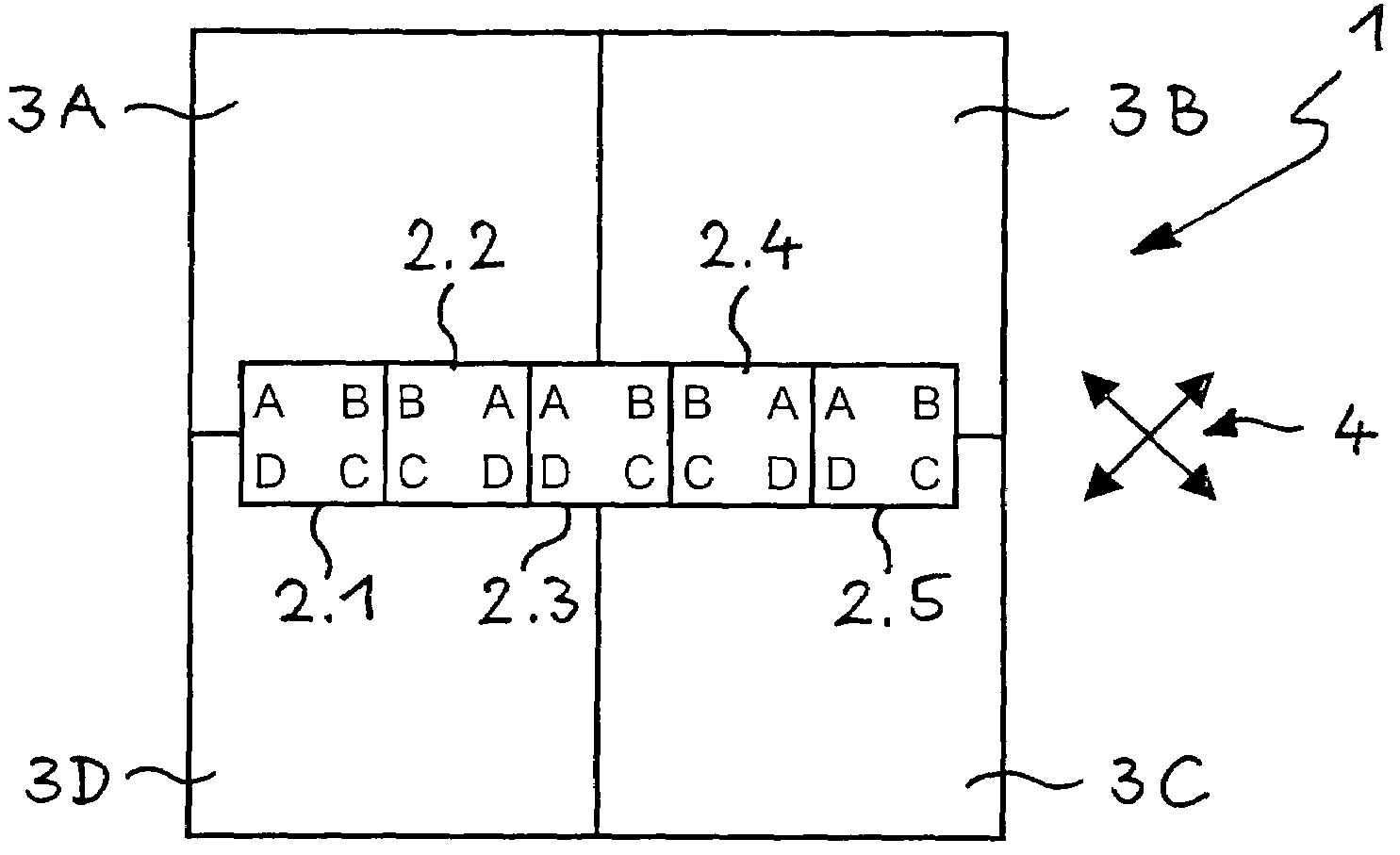
[0033]a pixel 1 according to the invention is depicted in FIG. 4. Five small-sized photo-sensitive areas 2.1-2.5 of rectangular or square shape are placed in a row. They are all interlinked to the four storage sites 3A-3D by appropriate transfer means for transferring the charge carriers to a common storage site, e.g., 3D. The storages sites 3A-3D and the output electronics are shared by all five small-sized photo-sensitive areas 2.1-2.5 of the pixel 1. Already here, an increase of both fill-factor and demodulation frequency is recognized when comparing the pixel arrangement with the prior-art pixel architecture of FIG. 3.

second embodiment

[0034]FIG. 5 illustrates the pixel 1 according to the invention. Several, e.g., nine, small-sized photo-sensitive areas 2.1-2.9 form a cross-like area on the pixel 1. The number of storage sites 3A-3D is four again.

[0035]FIG. 6 shows a pixel 1 with a two-dimensional array of, e.g., 3×3=9 small-sized photo-sensitive areas 2.1-2.9, delivering four samples each to a selected one, e.g., 3D, of four storage areas 3A-3D.

[0036]It is possible to design pixels 1 according to the invention with a plurality of photo-sensitive areas 2.1-2.6 delivering three samples. Such an embodiment is sketched in FIG. 7, where six small-sized photo-sensitive elements 2.1-2.6 transfer their charge carriers to a selected one of three common storage sites (not shown).

[0037]Preferred photo-sensitive elements 2, 2′ that allow controlling the transfer of photo-generated electrons to different storage sites are depicted in FIGS. 8 and 9, respectively. The invention is, however, not limited to these two presented de...


PUM


Abstract

The pixel (1) for use in an image sensor comprises a plurality of small-sized radiation-sensitive elements (2.1-2.9) for converting incident radiation into electric signals, the radiation-sensitive elements (2.1-2.9) being properly interconnected to form a larger radiation-sensitive area. The pixel (1) further comprises a plurality of storage elements (3A-3D) for storing the electric signals. The pixel further comprises transfer means for transferring the electric signals from the radiation-sensitive elements (2.1-2.9) to any selected one of the storage elements (3A-3D). The pixel (1) exhibits a high optical sensitivity and a high demodulation speed, and is especially suited for distance-measuring sensors based on the time-of-flight (TOF) principle or interferometry.

Description

[0001]This application claims priorty to European application No. 05 405 476.2 filed Aug. 12, 2005.FIELD OF THE INVENTION[0002]The present invention relates to solid-state photosensing and imaging, and especially to all solid-state photosensing applications demanding highly sensitive pixels coupled with extremely fast on-pixel samplings. These pixel characteristics are desired for spatially resolved photodetection and demodulation of temporally intensity-modulated electromagnetic waves. Such pixels are particularly interesting for non-contact distance-measuring sensors based on the time-of-flight (TOF) principle or interferometry, but as well for phase-measuring bio(chemical) applications such as fluorescence applications. The invention relates to all the sensing techniques that require one- or two-dimensional arrays of demodulation pixels.BACKGROUND OF THE INVENTION[0003]DE-44′40′613 C1 (Th. Sprig, P. Seitz; “Vorrichtung und Verfahren zur Detektion und Demodulation eines intensität...

Claims


Application Information

Patent Timeline
Patent Type & Authority Patents(United States)
IPC IPC(8): H01L27/146
CPCG01J3/2803H01L31/02024H01L27/14603
Inventor OGGIER, THIERRYLEHMANN, MICHAELBUTTGEN, BERNHARD
Owner AMS SENSORS SINGAPORE PTE LTD
Why Eureka
Try Eureka