Imaging member
a technology of imaging members and ions, applied in the field of imaging members, can solve the problems of affecting copy quality, surface cracking, photoreceptor surface cracking, etc., and achieve the effects of reducing and/or eliminating the presence of residual solvent, eliminating internal strain, and effectively flushing out residual solven
- Summary
- Abstract
- Description
- Claims
- Application Information
AI Technical Summary
Benefits of technology
Problems solved by technology
Method used
Image
Examples
control example i
[0143]An electrophotographic imaging member web was prepared by providing a 0.02 micrometer thick titanium layer coated on a substrate of a biaxially oriented polyethylene naphthalate substrate (KADALEX™, available from Dupont Teijin Films.) having a thickness of 3.5 mils (89 micrometers). The titanized Kadalex™ substrate was extrusion coated with a blocking layer solution containing a mixture of 6.5 grams of gamma aminopropyltriethoxy silane, 39.4 grams of distilled water, 2.08 grams of acetic acid, 752.2 grams of 200 proof denatured alcohol and 200 grams of heptane. This wet coating layer was then allowed to dry for 5 minutes at 135° C. in a forced air oven to remove the solvents from the coating and effect the formation of a crosslinked silane blocking layer. The resulting blocking layer was of an average dry thickness of 0.04 micrometer as measured with an ellipsometer.
[0144]An adhesive interface layer was then applied by extrusion coating to the blocking layer with a coating so...
control example ii
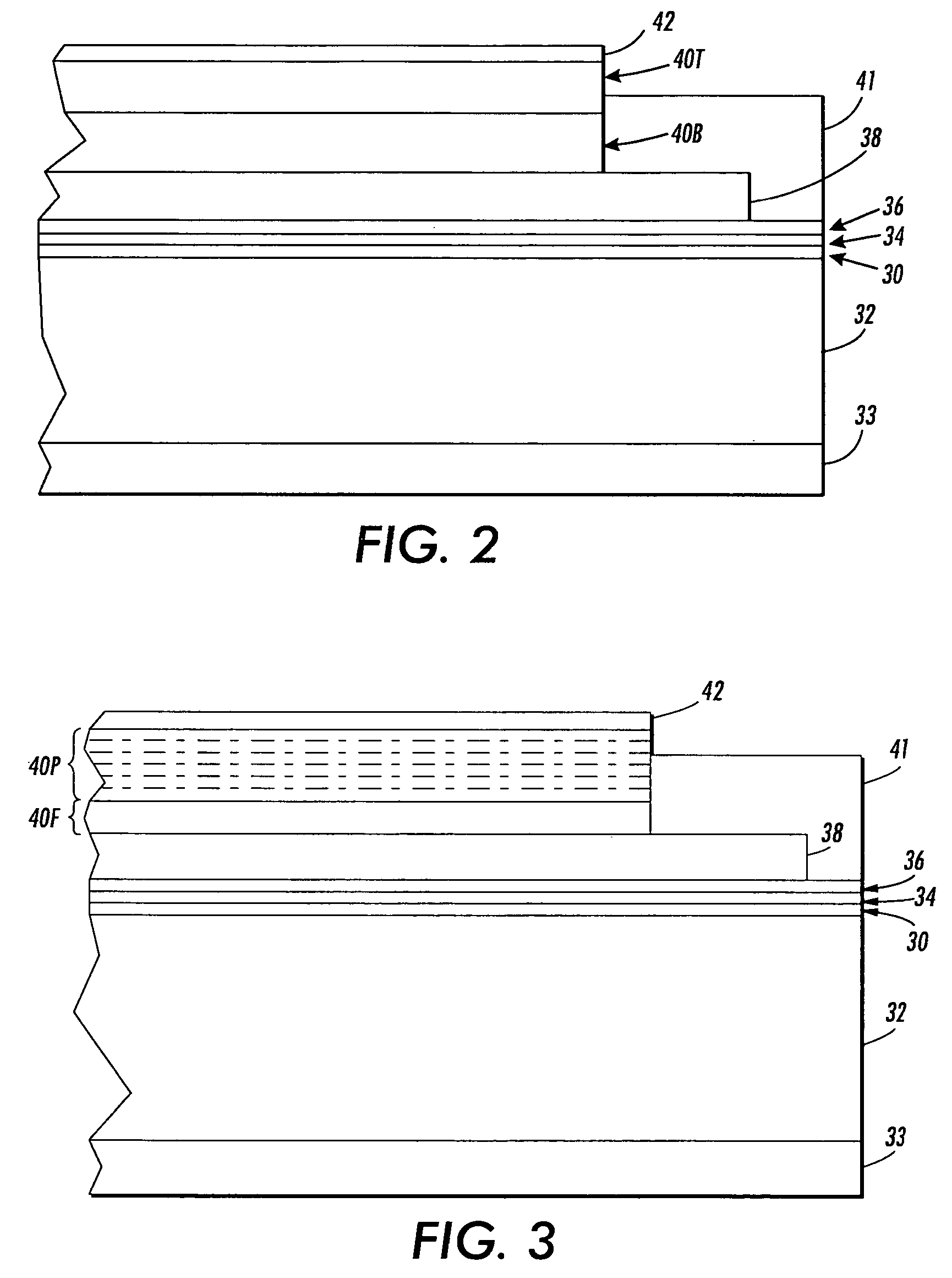
[0152]An electrophotographic imaging member web was prepared in exactly the manner and using the same materials as those described in Control Example I, but with the exception that the charge transport layer was prepared to give dual charge transport layers consisting of a bottom charge transport layer and a top charge transport layer.
[0153]In essence, the above coated imaging member web was then coated over with two separate charge transport layers and a ground strip layer using an extrusion co-coating process. Both charge transport layers were prepared by two separate coating solutions by introducing into an amber glass bottle the N,N′-diphenyl-N,N′-bis(3-methylphenyl)-1,1′-biphenyl-4,4′-diamine hole transporting compound and MAKROLON® 5705, a Bisphenol A polycarbonate, poly(4,4′-isopropylidene diphenyl) carbonate, having a weight average molecular weight of about 120,000 and available from Bayer A G, was added to the glass bottle to make up two separate charge transport layer coa...
example i
Disclosure Example I
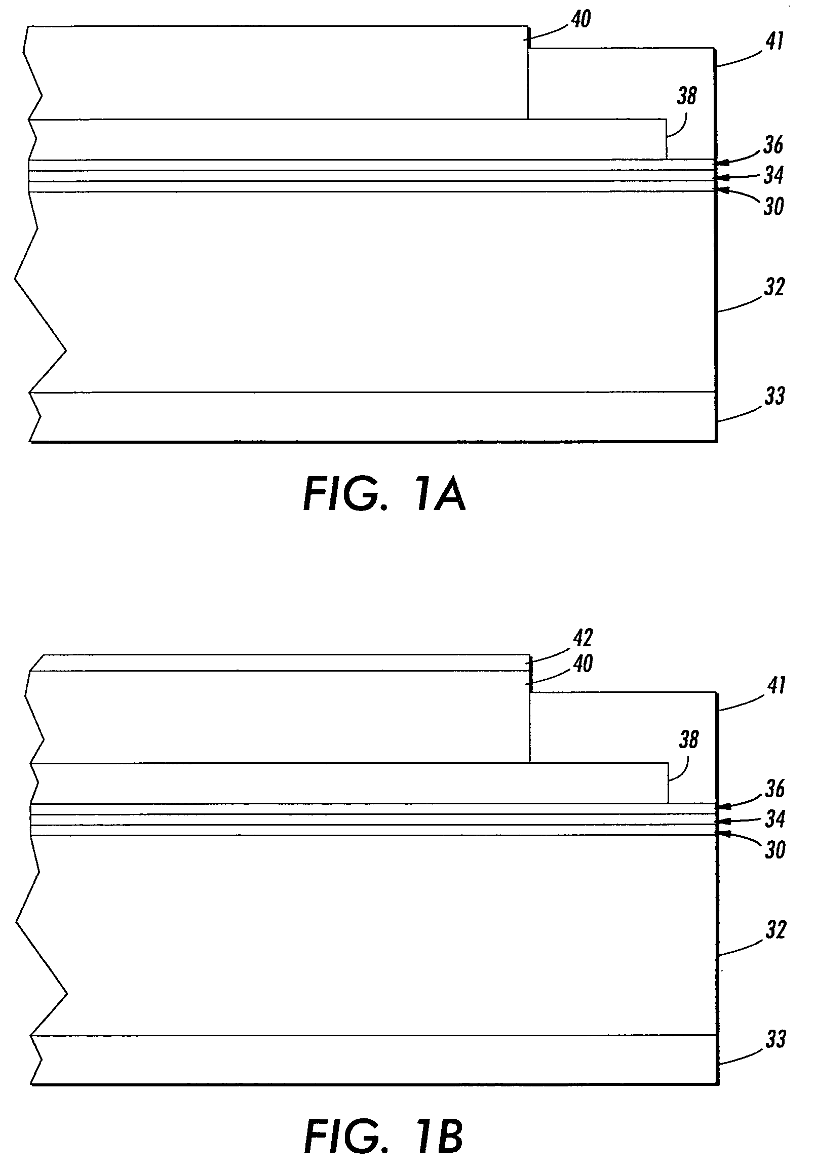
[0156]Two electrophotographic imaging member webs (each having a single charge transport layer shown in FIG. 1A) were fabricated using the same materials and the same process as that described in the Control Example I, but with the exception that the charge transport layer coating solutions were prepared to include a high boiler Bisphenol A carbonate monomer liquid (boiling point of about 300° C.), in three different amounts, given by Formula (IV) below:
[0157]
[0158]Since this liquid compound is a Bisphenol A bisallyl carbonate monomer (commercially available for PPG, Inc.) to that of polycarbonate Makrolon® 5705 binder, it presence in any amount should have good compatible with the material compositions of the formulated charge transport layer.
[0159]The prepared first charge transport layer coating solution was then applied onto the charge generating layer and followed by subsequent drying at elevated temperature to give the resulting imaging member web stocks wh...
PUM
| Property | Measurement | Unit |
|---|---|---|
| thickness | aaaaa | aaaaa |
| thickness | aaaaa | aaaaa |
| temperature | aaaaa | aaaaa |
Abstract
Description
Claims
Application Information


