Light-emitting device and method for manufacturing the same
a technology of light-emitting devices and manufacturing methods, which is applied in the direction of semiconductor devices, electrical devices, transistors, etc., can solve the problems of waste of material resources, large quantity of effluent disposal, and difficulty in manufacturing a display panel with good productivity and low cost by a conventional patterning method, so as to improve material efficiency and simplify manufacturing steps , the effect of preventing deterioration
- Summary
- Abstract
- Description
- Claims
- Application Information
AI Technical Summary
Benefits of technology
Problems solved by technology
Method used
Image

Examples
embodiment mode 1
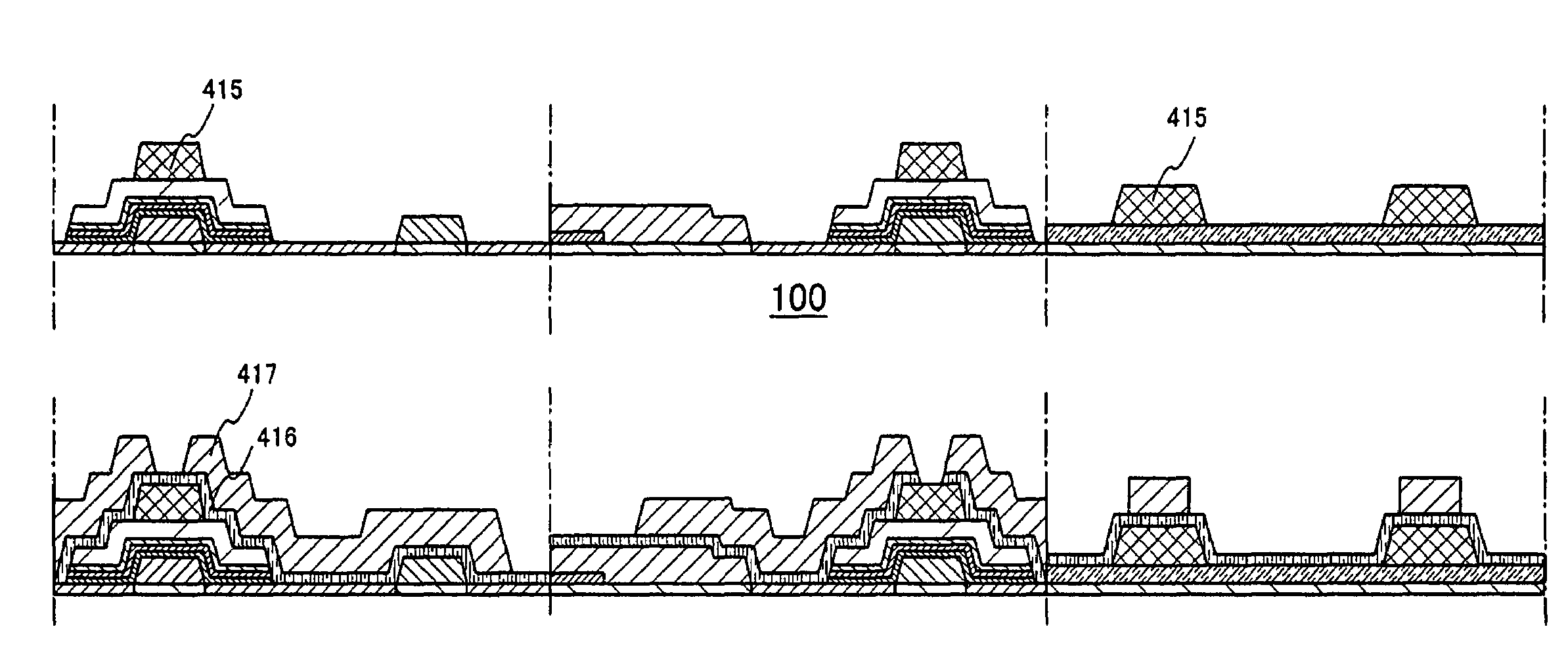
[0073]A method for manufacturing a channel protective type TFT is explained in Embodiment mode 1.
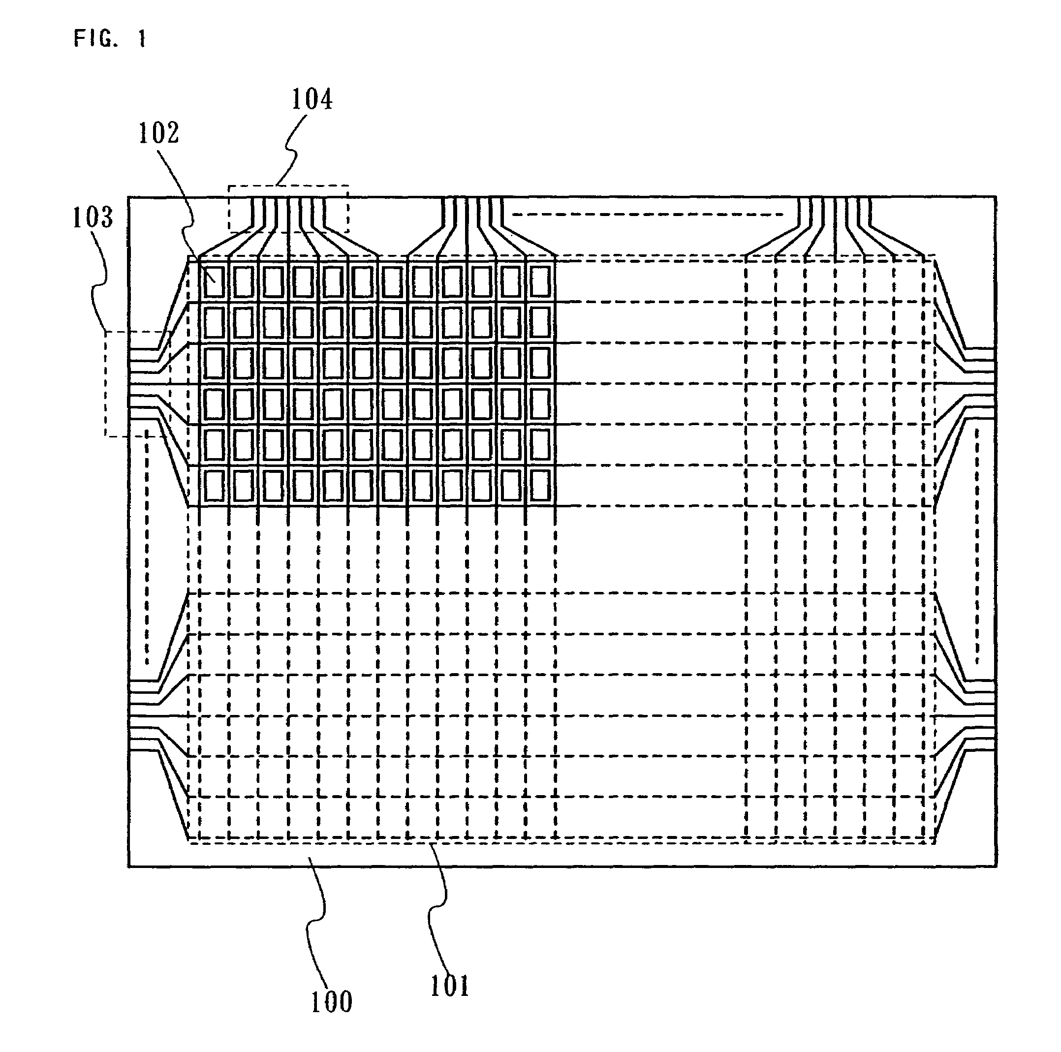
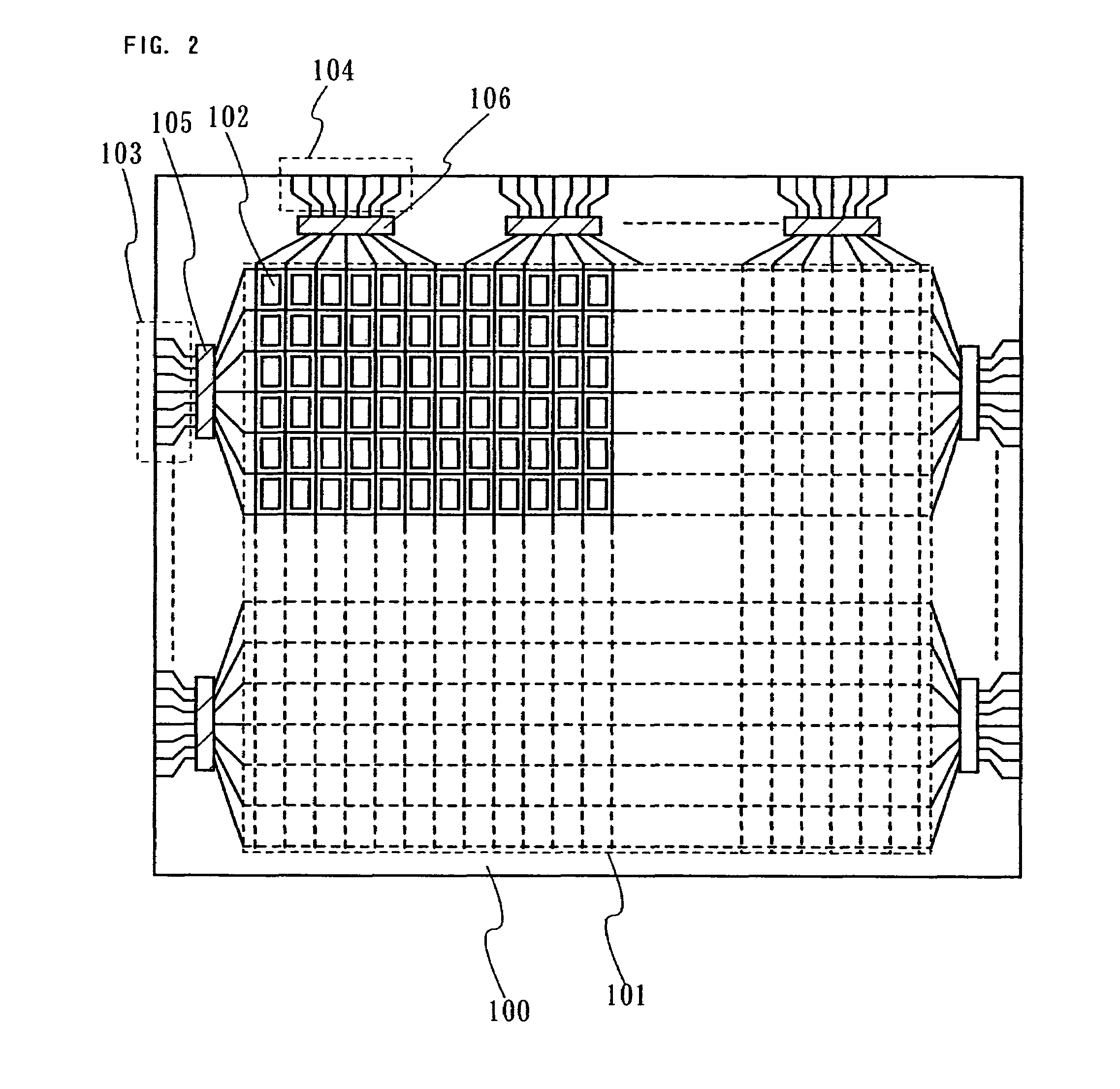
[0074]FIG. 4A shows a step of forming a gate electrode, and a gate wiring connected to the gate electrode over a substrate 100 by a droplet discharging method. Note that FIG. 4A shows a longitudinal sectional structure schematically, and FIG. 8 shows a planar structure corresponding to a-b, c-d and e-f thereof, and thus, the figures can be referred to at the same time.
[0075]A plastic substrate having the heat resistance that can withstand processing temperature of the manufacturing step, or other substrates can be used for the substrate 100, in addition to a non-alkaline glass substrate such as barium borosilicate glass, alumino borosilicate glass, or aluminosilicate glass manufactured with a fusion method or a floating method, and a ceramic substrate. A semiconductor substrate such as single crystal silicon, a substrate in which a surface of a metal substrate such as stainless is provid...
embodiment mode 2
[0105]A method for manufacturing a channel etch type TFT is explained in Embodiment mode 2.
[0106]A base film 201 is formed on a substrate 100, and a gate wiring 202, gate electrodes 203 and 204 are formed over the base film 201 by discharging a composition including a conductive material. After the gate wiring 202, the gate electrodes 203 and 204 are formed, the exposed base film 201 in the surface is treated and insulated to form an insulating layer 205 or removed by etching using the gate wiring 202, the gate electrodes 203 and 204 as a mask. Then, a gate insulating layer 206 is formed by plasma CVD or sputtering to have a single layer structure or a laminated layer structure. More preferably, a lamination of three layers, an insulating layer 207 of silicon nitride, an insulating layer 208 of silicon oxide and an insulating layer 209 of silicon nitride serves as the gate insulating layer. Further, a semiconductor film 210 serving as an active layer is formed. A mask 211 is formed ...
embodiment mode 3
[0109]A method for manufacturing a channel protective type TFT in which a first electrode is formed over a base film is explained in Embodiment mode 3.
[0110]FIG. 9A shows a step of forming a first electrode over a substrate 100, and FIG. 9B shows a step of forming a gate electrode, and a gate wiring connected to the gate electrode by a droplet discharging method. Note that FIG. 9A shows schematically a longitudinal sectional structure, and FIG. 13 shows a planar structure corresponding to a-b, c-d and e-f thereof, and thus, the figures can be referred to at the same time.
[0111]A plastic substrate having the heat resistance that can withstand processing temperature of the manufacturing step or the like can be used for the substrate 100, in addition to a non-alkaline glass substrate such as barium borosilicate glass, alumino borosilicate glass, or aluminosilicate glass manufactured by a fusion method or a floating method, and a ceramic substrate. In addition, a semiconductor substrate...
PUM
 Abstract
Description
Claims
Application Information
 - R&D
- Intellectual Property
- Life Sciences
- Materials
- Tech Scout
- Unparalleled Data Quality
- Higher Quality Content
- 60% Fewer Hallucinations
Browse by: Latest US Patents, China's latest patents, Technical Efficacy Thesaurus, Application Domain, Technology Topic, Popular Technical Reports.
© 2025 PatSnap. All rights reserved.Legal|Privacy policy|Modern Slavery Act Transparency Statement|Sitemap|About US| Contact US: help@patsnap.com