Process for forming high resistivity thin metallic film

Inactive Publication Date: 2010-06-03
ASM JAPAN
View PDF22 Cites 96 Cited by
  • Summary
  • Abstract
  • Description
  • Claims
  • Application Information

AI Technical Summary

Benefits of technology

[0013]In one embodiment, a conductive metal nitride thin film is provided with a resistivity between 1,000 μΩcm and 15,000 μΩcm. The thickness non-uniformity (NU) across the substrate can be less than 1%, and resistivity non-uniformity (Rs NU)

Problems solved by technology

However, the resistivity of polycrystalline silicon has a high sensitivity to temperature, which is not suitable for analog circuits, and the resistivity of the resistors using silicon tends to be relatively low.
Another issue is controllability and accuracy of the sheet resistance (resistivity/film thickness).
However, this process has been found to be i

Method used


Image

  • Process for forming high resistivity thin metallic film
  • Process for forming high resistivity thin metallic film
  • Process for forming high resistivity thin metallic film

Examples


Example

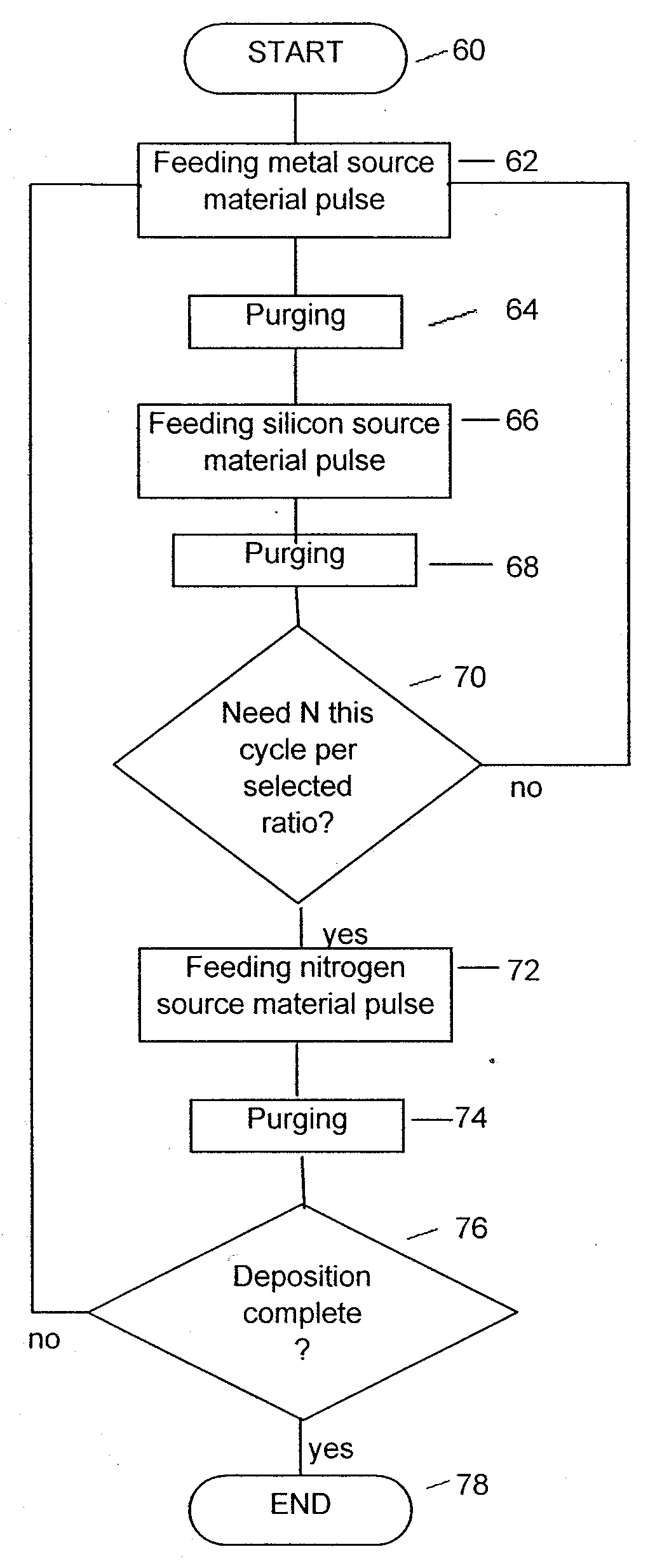
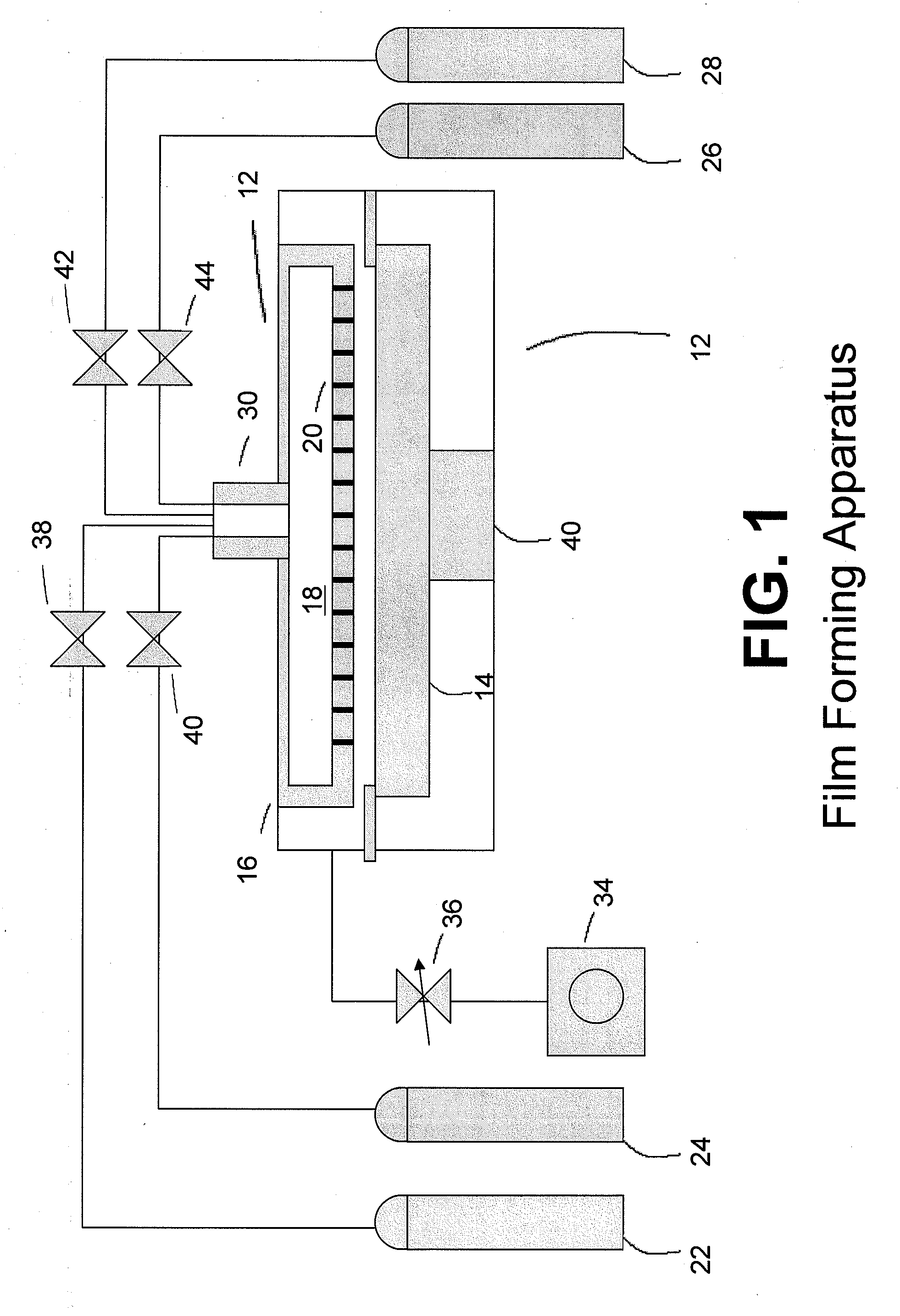
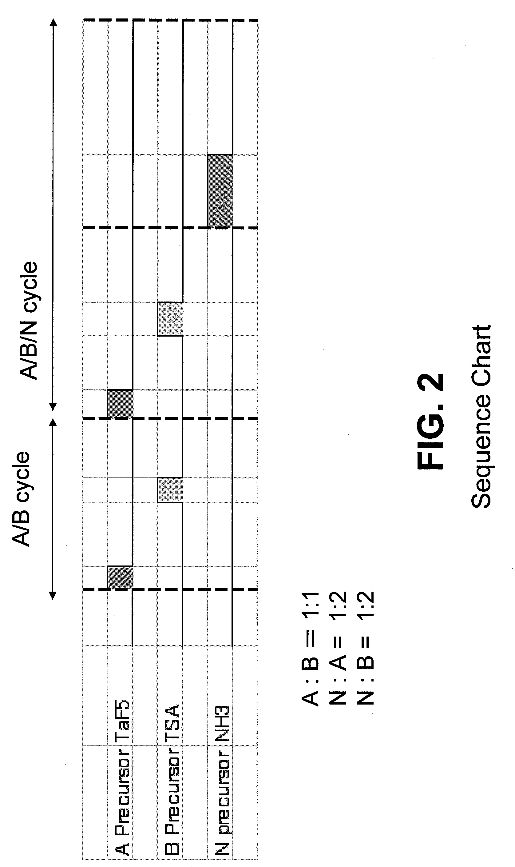
[0020]As shown in FIG. 1, ALD apparatus according to one embodiment comprises a reaction chamber 12 equipped with a susceptor 14 for supporting a substrate within under a showerhead 16 or other gas inlet structure. The susceptor 14 can be heated in a variety of manners, such as internal resistive heating coils. The showerhead 16 contains a cavity known as a showerhead plenum 18 and showerhead plate 20, which has openings for supplying gases to the substrate. Process gas sources communicate with the inlet structure or showerhead 16. In the illustrated embodiment, the gas sources include a metal precursor source 22, a silicon precursor source 24, a nitrogen precursor source 26 and a source of inert or purge gas 28. The process gas sources 22-28 communicate with the showerhead plenum 18 through an inlet 30 and the showerhead plate 20 provides some backpressure to spread the gases across the plenum 18 and feed gas downward uniformly through multiple holes. A pedestal 32 supports the sus...


PUM

PropertyMeasurementUnit
Thicknessaaaaaaaaaa
Fractionaaaaaaaaaa
Electrical resistivityaaaaaaaaaa

Abstract

A process for forming metallic nitride film by atomic layer deposition (ALD), which comprises steps for feeding into a reaction space vapor phase alternated pulses of metal source material and silicon source material in a plurality of cycles, and feeding into the reaction space vapor phase pulses of nitrogen source material. wherein a nitrogen source pulse is fed intermittently in selected cycles such that a ratio of nitrogen source pulses to silicon source pulses is less than 1:1 and a ratio of nitrogen source pulses to metal source pulses is less than 1:1, the ratio selected to produce the thin film with a resistivity between 1,000 μΩcm and 15,000 μΩcm.

Description

BACKGROUND OF THE INVENTION[0001]1. Field of the Invention[0002]The present invention relates to a process for forming thin metal film, more particularly, the present invention relates to a process for forming metal nitride thin film by atomic layer deposition (ALD), controlling the resistivity thereof.[0003]2. Description of the Related Art[0004]Tantalum Nitride (TaN) thin films have been used as barrier films in metallization for integrated circuits. Additionally, tantalum silicon nitride compounds (TaSiN) have been described as useful for transistor gate electrode applications. For example, U.S. Pat. No. 6,518,106 describes that gate electrode and electrode work function can be tuned by the concentration of nitrogen in tantalum silicon nitride (TaSiN).[0005]The resistivity is one of the critical material properties to control for various layers used in making semiconductor devices. Normally the resistivity is mostly determined by the material itself. A thin film resistor is usefu...

Claims


Application Information

Patent Timeline
IPC IPC(8): C23C16/34B32B9/00C01B33/00
CPCC01B33/00C23C16/45531C23C16/34
Inventor SHIMIZU, AKIRAKOBAYASHI, AKIKOHAUKKA, SUVI
Owner ASM JAPAN
Why Eureka
Try Eureka