Stress-managed revision of integrated circuit layouts

a technology of integrated circuits and layouts, applied in the direction of cad circuit design, computer aided design, instruments, etc., can solve the problems of degrading other performance measures, reducing the performance of other performance measures, and continuing shrinkage of technology

US7600207B2Active Publication Date: 2009-10-06SYNOPSYS INC
18 Cites 24 Cited by

Patent Information

Authority / Receiving Office
US · United States
Patent Type
Patents(United States)
Current Assignee / Owner
Publication Date
2009-10-06

Smart Images

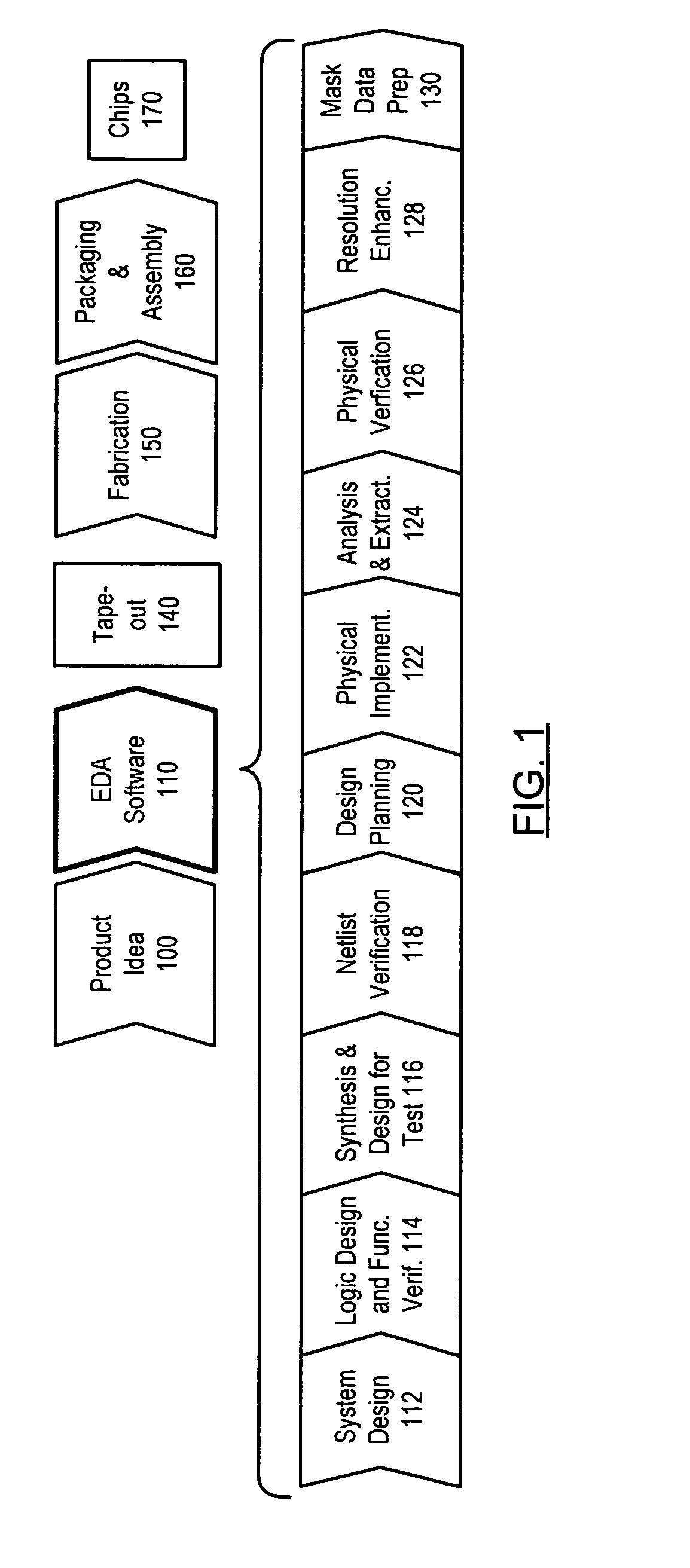
  • Figure 1
    Figure 1
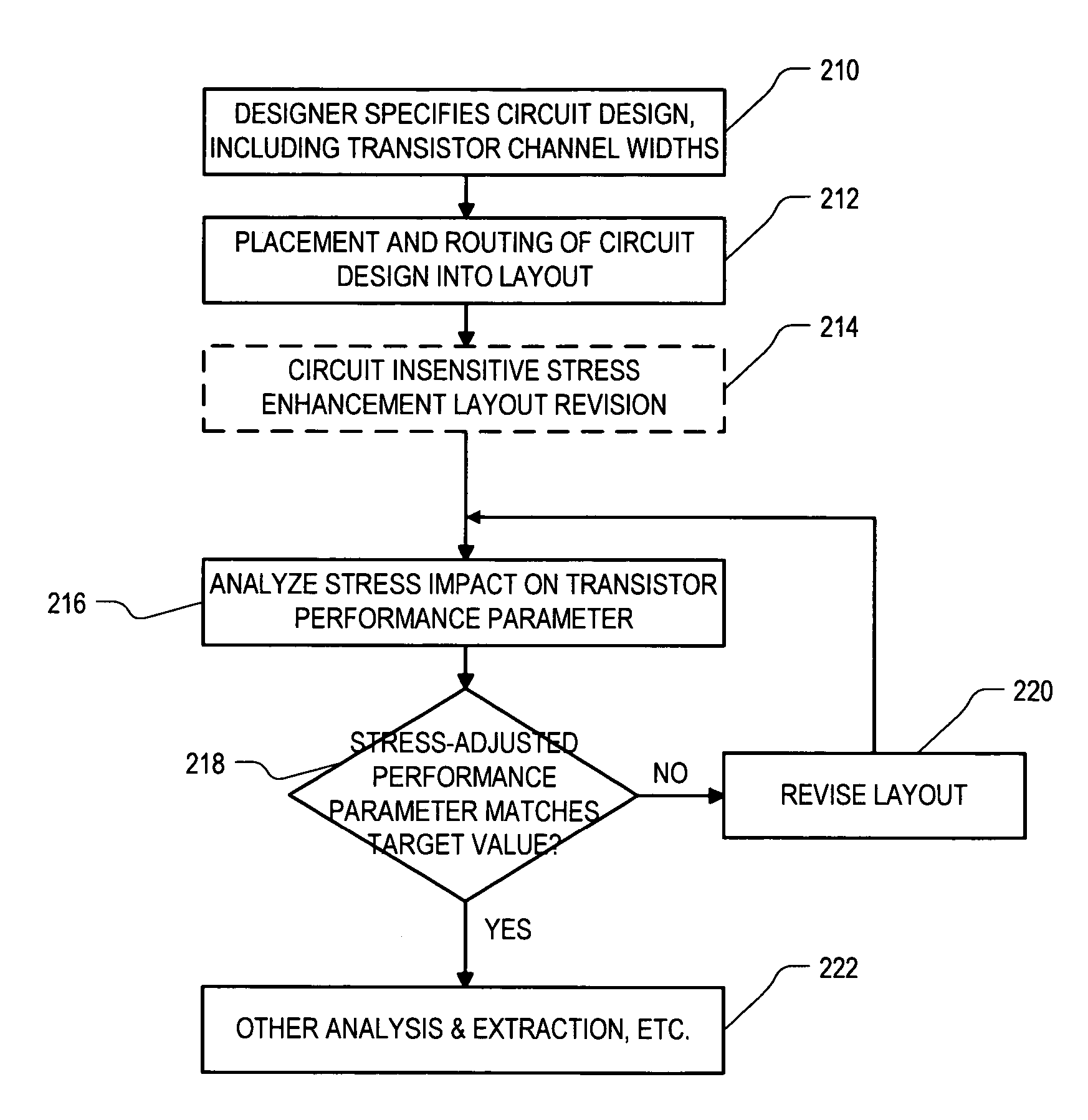
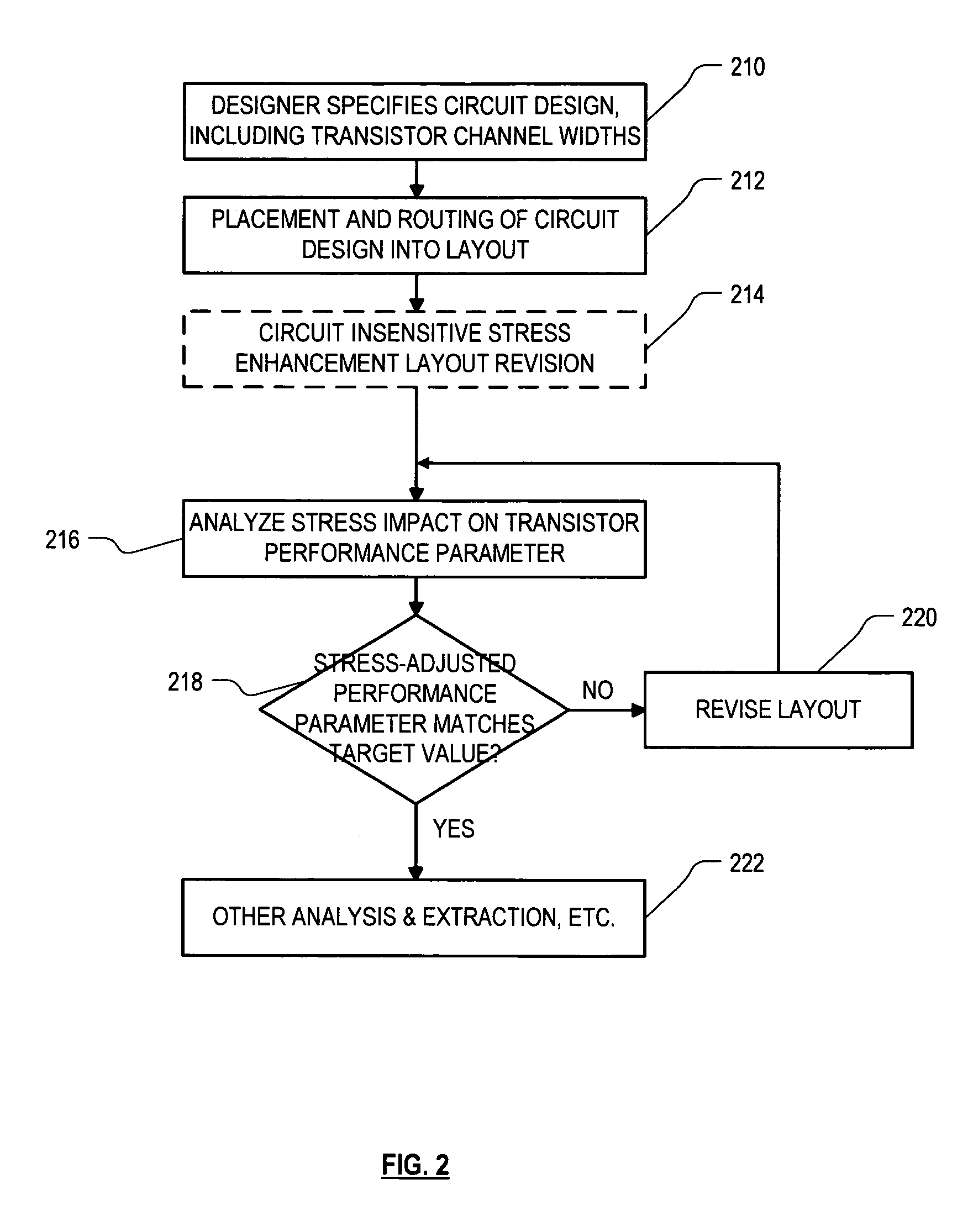
  • Figure 2
    Figure 2
  • Figure 3
    Figure 3
Patent Text Reader

Abstract

Roughly described, methods and systems for improving integrated circuit layouts and fabrication processes in order to better account for stress effects. Dummy features can be added to a layout either in order to improve uniformity, or to relax known undesirable stress, or to introduce known desirable stress. The dummy features can include dummy diffusion regions added to relax stress, and dummy trenches added either to relax or enhance stress. A trench can relax stress by filling it with a stress-neutral material or a tensile strained material. A trench can increase stress by filling it with a compressive strained material. Preferably dummy diffusion regions and stress relaxation trenches are disposed longitudinally to at least the channel regions of N-channel transistors, and transversely to at least the channel regions of both N-channel and P-channel transistors. Preferably stress enhancement trenches are disposed longitudinally to at least the channel regions of P-channel transistors.
Need to check novelty before this filing date? Find Prior Art

Description

FIELD OF THE INVENTION

[0001] The invention relates to methods and systems for improving integrated circuit performance through stress-engineering of the layout, and articles manufactured thereby.INTRODUCTION

[0002] It has long been known that semiconductor materials such as silicon and germanium exhibit the piezoelectric effect (mechanical stress-induced changes in electrical resistance). See for example C. S. Smith, “Piezoresistance effect in germanium and silicon”, Phys. Rev., vol. 94, pp. 42-49 (1954), incorporated by reference herein. The piezoelectric effect has formed the basis for certain kinds of pressure sensors and strain gauges, but only recently has it received attention in the manufacture of integrated circuits. In integrated circuit fabrication, one of the major sources of mechanical stress is the differential expansion and contraction of the different materials used. For example, typical fabrication technologies involve electrically isolating the active regions of groups...

Examples

Embodiment Construction

[0030]The following description is presented to enable any person skilled in the art to make and use the invention, and is provided in the context of a particular application and its requirements. Various modifications to the disclosed embodiments will be readily apparent to those skilled in the art, and the general principles defined herein may be applied to other embodiments and applications without departing from the spirit and scope of the present invention. Thus, the present invention is not intended to be limited to the embodiments shown, but is to be accorded the widest scope consistent with the principles and features disclosed herein.

[0031]FIG. 1 shows a simplified representation of an illustrative digital integrated circuit design flow. At a high level, the process starts with the product idea (step 100) and is realized in an EDA (Electronic Design Automation) software design process (step 110). When the design is finalized, it can be taped-out (step 140). After tape out, ...