
Monolithic ceramic electronic component and method for manufacturing the same

a technology of electronic components and monolithic ceramics, applied in the direction of variable capacitors, fixed capacitor details, fixed capacitors, etc., can solve the problems of poor plating, easy deterioration of weather resistance, etc., to achieve satisfactory electrical connection reliability, not to cause deterioration of insulation resistance, and satisfactory solderability of external electrodes

Inactive Publication Date: 2009-11-03
MURATA MFG CO LTD
View PDF10 Cites 3 Cited by
  • Summary
  • Abstract
  • Description
  • Claims
  • Application Information

AI Technical Summary

Benefits of technology

[0016]In order to overcome the problems described above, preferred embodiments of the present invention provide a monolithic ceramic electronic component, wherein intrusion of the plating solution into a ceramic laminate can be suppressed and prevented so as not to cause deterioration of the insulation resistance and the deterioration of the weather resistance, and satisfactory reliability of electrical connection between an external electrode and internal electrodes and satisfactory solderability of the external electrode are achieved, as well as a method for manufacturing the monolithic ceramic electronic component.

Problems solved by technology

As a result, when the external electrode is subjected to Ni plating or Sn plating, a plating solution is liable to intrude into the ceramic laminate and, thereby, deterioration of the insulation resistance and deterioration of the weather resistance occur easily.
If the amount of addition of the glass to the electrically conductive paste for forming the external electrode is increased, there are problems in that, for example, poor plating occurs as a result of rising (excessive deposition) of glass to the external electrode surface.

Method used


Image

  • Monolithic ceramic electronic component and method for manufacturing the same
  • Monolithic ceramic electronic component and method for manufacturing the same
  • Monolithic ceramic electronic component and method for manufacturing the same

Examples


example 1

[0069]A monolithic ceramic capacitor (Sample Nos. 1 to 11), as described below, was produced as a monolithic ceramic electronic component, and characteristics thereof were examined.

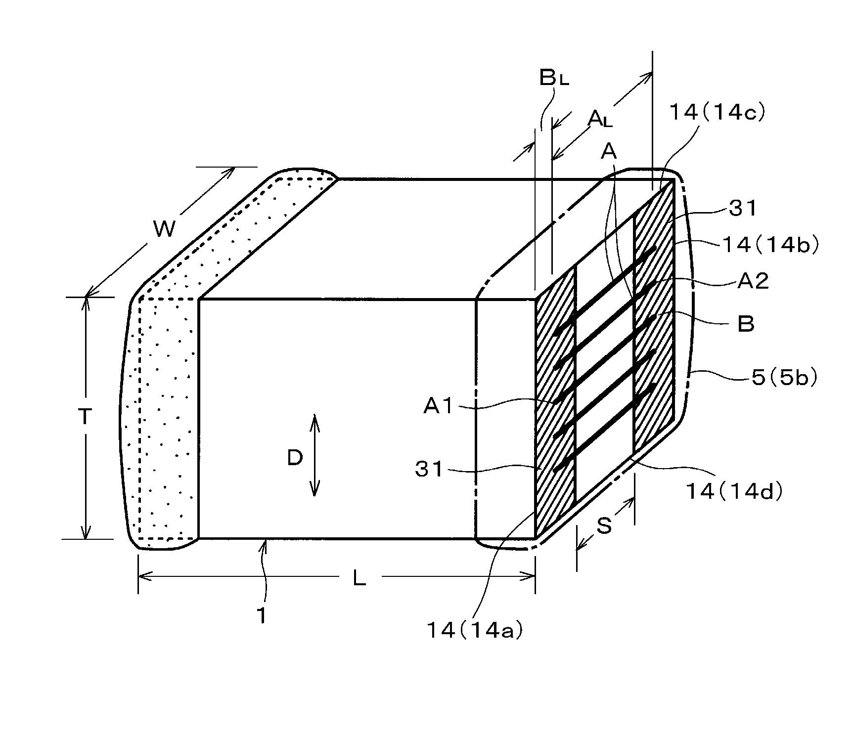
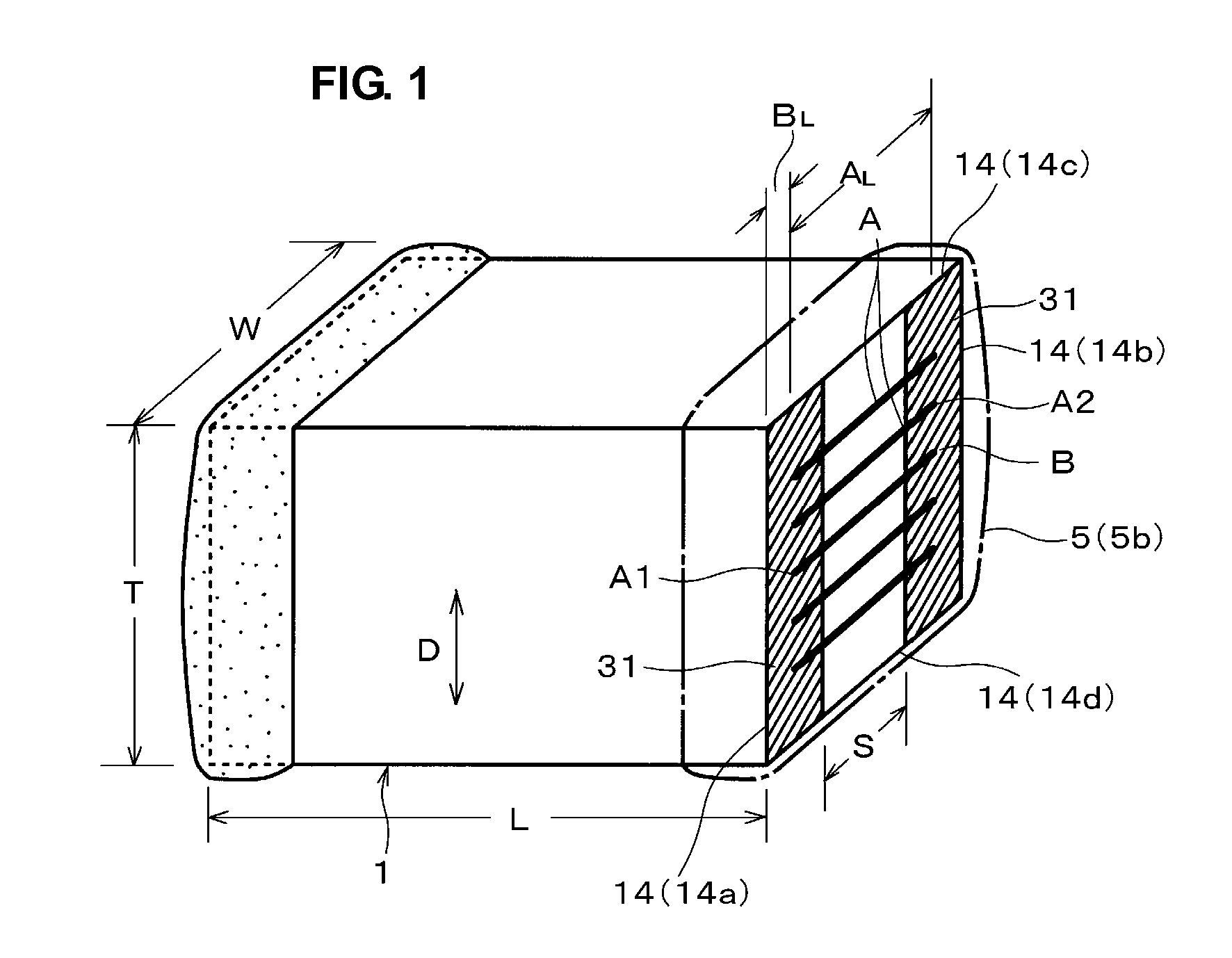
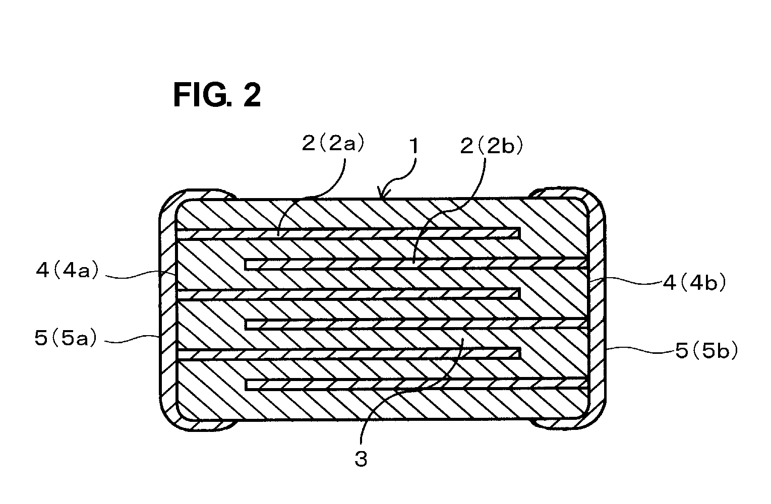
[0070]The monolithic ceramic capacitor produced in Example 1 is a monolithic ceramic capacitor having a structure in which, as shown in FIG. 1 and FIG. 2, a plurality of internal electrode layers 2 (2a, 2b) are disposed opposite to each other with ceramic layers 3 therebetween while being alternately led to opposite end surfaces 4 (4a, 4b) so as to constitute a ceramic laminate 1, and a pair of external electrodes 5 (5a, 5b) are disposed on the two end portions of the ceramic laminate 1 so as to connect to the internal electrode layers 2 (2a, 2b), as a basic structure.

[0071]A production method and a structure of each sample (monolithic ceramic capacitor) and an evaluation of characteristics will be described below.

Production of Sample Nos. 1 to 4

1) Production of Ceramic Laminate

[0072]Ceramic green sheets ...

example 2

[0114]FIG. 10 and FIG. 11 are diagrams showing key portions of a monolithic ceramic electronic component (monolithic ceramic capacitor) according to another example (Example 2) of preferred embodiments of the present invention.

[0115]As shown in FIG. 10 and FIG. 11, in the monolithic ceramic electronic component of Example 2, among a plurality of internal electrode layers 2 exposed at an end surface 4 of a ceramic laminate 1, only both end portions in a longitudinal direction of the exposed portions of the uppermost internal electrode layer 102a and the lowermost internal electrode layer 102b are covered with glass films 31, and the other portions are not specifically covered with the glass film.

[0116]With respect to the configuration of Example 2 in which only both end portions in the longitudinal direction of the exposed portions of the uppermost internal electrode layer 102a and the lowermost internal electrode layer 102b are covered with glass films 31, as described above, since ...


PUM

PropertyMeasurementUnit
capacitanceaaaaaaaaaa
lengthaaaaaaaaaa
lengthaaaaaaaaaa

Abstract

A monolithic ceramic electronic component includes a ceramic laminate provided with ceramic layers and internal electrode layers disposed between the ceramic layers such that a portion of each internal electrode is led to an end surface of the ceramic laminate and the external electrode disposed on the end surface of the ceramic laminate to which the internal electrode layers are led, so as to connect to the internal electrode layers. At least one end portion in a longitudinal direction of an exposed portion of the internal electrode layer led to and exposed at the end surface of the ceramic laminate is covered with a glass film, and the internal electrodes and the external electrode are electrically connected to each other at a portion not covered with the glass film in the exposed portion of the internal electrode layer.

Description

BACKGROUND OF THE INVENTION[0001]1. Field of the Invention[0002]The present invention relates to a monolithic ceramic electronic component and a method for manufacturing the same. In particular, the present invention relates to a monolithic ceramic electronic component having a structure in which internal electrodes are disposed between ceramic layers such that a portion of each internal electrode is led to an end surface and an external electrode is disposed on an end surface of a ceramic laminate so as to connect to the internal electrode layers, as well as a method for manufacturing the monolithic ceramic electronic component.[0003]2. Description of the Related Art[0004]In general, a surface mount monolithic ceramic capacitor that is a typical monolithic ceramic electronic component has a structure in which, as shown in FIG. 15, a plurality of internal electrode layers 52 (52a, 52b) are disposed opposite to each other with ceramic layers 53 therebetween while being alternately le...

Claims


Application Information

Patent Timeline
Patent Type & Authority Patents(United States)
IPC IPC(8): H01G4/228H01G4/06H01G4/12H01G4/232H01G4/30
CPCH01G4/232H01G4/30Y10T29/435
Inventor MAEGAWA, KIYOTAKAKUSANO, MITSUHIRO
Owner MURATA MFG CO LTD
Learn More