Cracks in a ceramic body due to stress in a plated layer of an external electrode in the ceramic electronic component cause problems.
Specifically, when there is large tensile stress in the plated layer of the external electrode, in mounting a completed ceramic electronic component on a substrate by
reflow soldering, a crack originating from the vicinity of an edge of the external electrode may be produced in the ceramic body.
When there is large tensile stress in the plated layer of the external electrode, the external electrode cannot sufficiently absorb expansion and contraction of the substrate and
cracking may be produced in the ceramic body.
In an example where there is large tensile stress in the plated layer of the external electrode, when the substrate is warped after the completed ceramic electronic component is mounted on the substrate, a crack originating from the vicinity of an edge of the external electrode may be produced in the ceramic body.
In this case again, due to large tensile stress in the plated layer of the external electrode, the external electrode cannot sufficiently absorb warpage of the substrate and
cracking may be produced in the ceramic body.
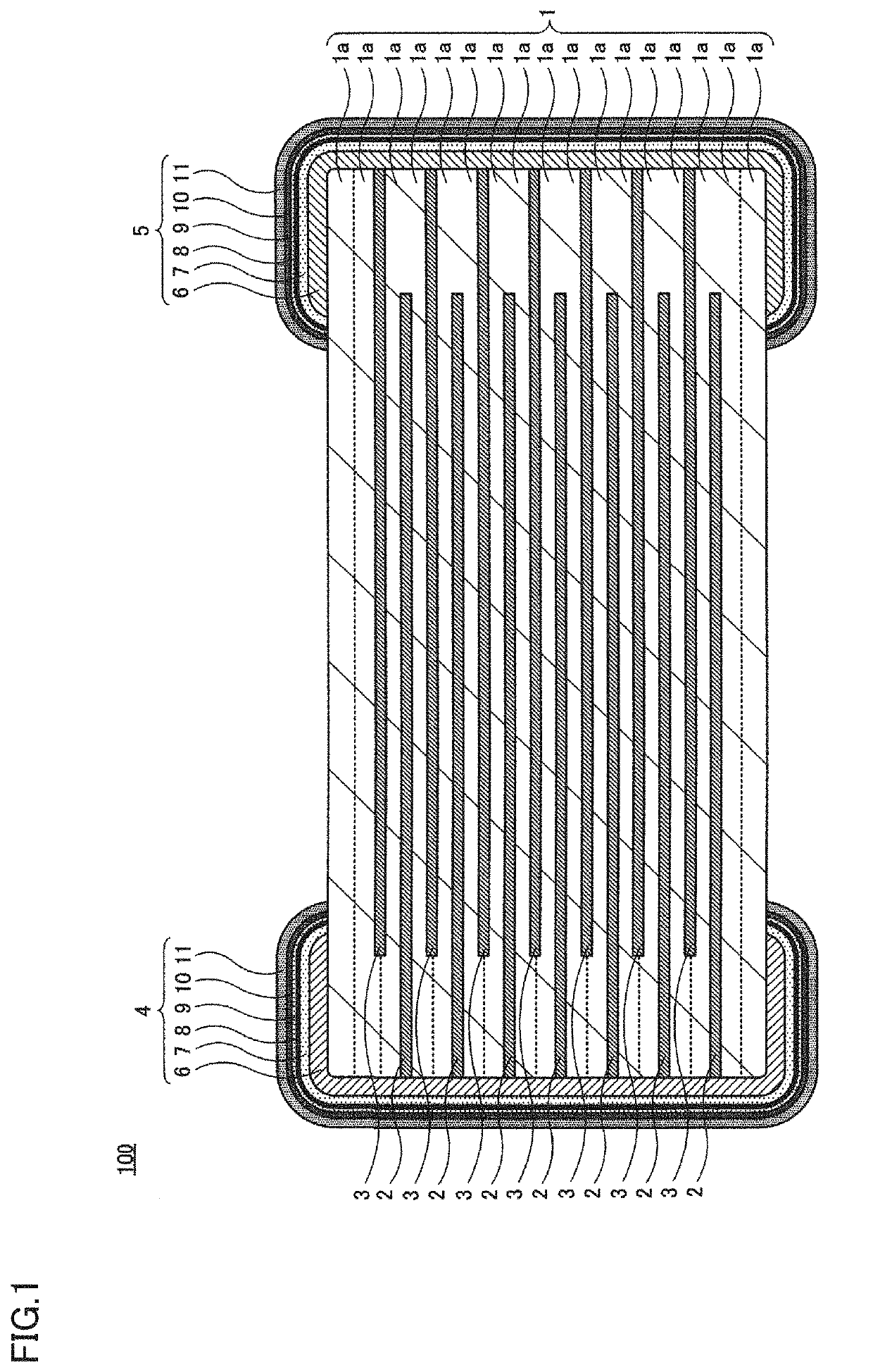
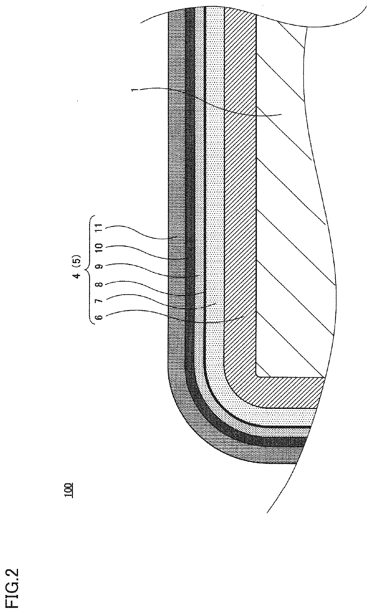
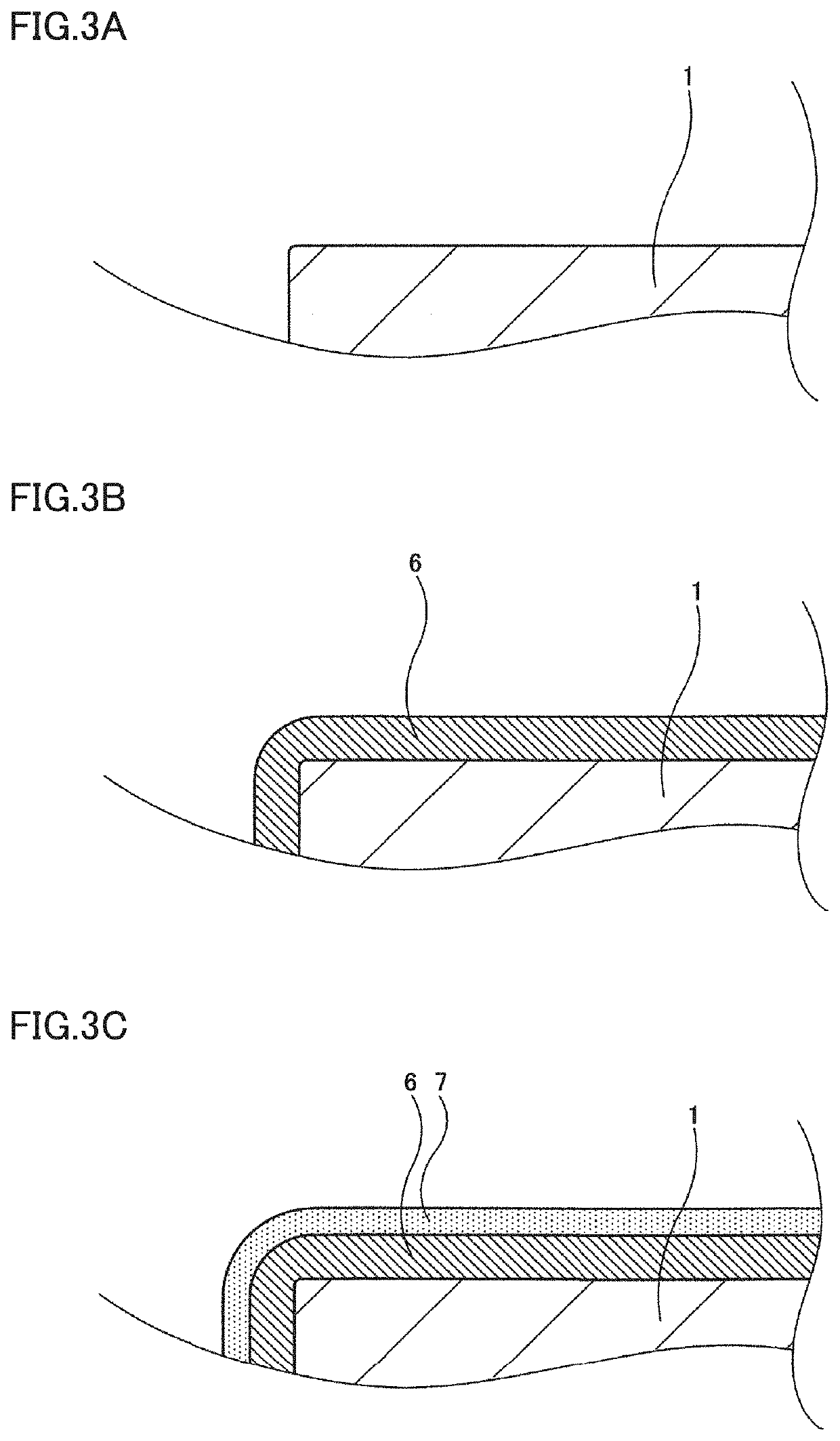
In an example where the external electrode includes an underlying electrode layer, an Ni plated layer, and an Sn plated layer, in connection with
cracking in the ceramic body due to stress in the plated layer, stress in the Ni plated layer particularly gives rise to a problem.
The multilayer ceramic
capacitor in Japanese Patent Laid-Open No. 2002-170733, however, suffers from a new problem of interfering with satisfactory solder mounting due to lowering in
solderability of the external electrode caused by the addition of the stress relaxing agent to the Ni plating bath, which will briefly be described below.
Specifically, in solder mounting (solder mounting by
reflow soldering) of a ceramic electronic component on a substrate, solder or a solder-Sn
alloy formed of solder and Sn in the Sn plated layer exhibits excellent wettability to a portion where the Ni—Sn
alloy layer is formed, whereas it does not exhibit satisfactory wettability to a portion where the Ni—Sn
alloy layer is not formed (a portion where the Ni—Sn alloy layer is not formed due to influence of later-described
Ni oxide formed on the outer surface of the Ni plated layer).
Therefore, unless an Ni—Sn alloy layer having a uniform thickness is formed between the Ni plated layer and the Sn plated layer, solder or a solder-Sn alloy does not satisfactorily spread in a
liquid state in that portion.
Then, a satisfactory solder fillet is not formed and joining of a ceramic electronic component to a substrate by solder may not be satisfactory.
Therefore, even though a small amount of
Ni oxide may be formed on the outer surface of the Ni plated layer, Ni
oxide in such an amount that gives rise to a problem is not formed.
Then, in the multilayer ceramic
capacitor in Japanese Patent Laid-Open No. 2002-170733, since Ni
oxide is formed on the outer surface of the Ni plated layer, the Ni
oxide interferes with formation of the Ni—Sn alloy layer having a uniform thickness between the Ni plated layer and the Sn plated layer in
spite of formation of the Sn plated layer on the outer side of the Ni plated layer.
Specifically, by adding the stress relaxing agent to the Ni plating bath for forming the Ni plated layer, Ni oxide is formed on the outer surface of the Ni plated layer and the Ni—Sn alloy layer having a uniform thickness is not formed between the Ni plated layer and the Sn plated layer, solder (a solder-Sn alloy) does not spread in a
liquid state in solder mounting, and joining of a ceramic electronic component to a substrate by solder may be defective.

