
Electronic component, mounting structure of electronic component

a technology of electronic components and mounting structures, applied in the direction of fixed capacitor details, printed circuit non-printed electric components association, capacitor manufacture, etc., can solve the problems of reducing the resistance of multi-layer ceramic capacitors mounted on mounting objects such as circuit boards, and deteriorating reliability, and achieve the effect of satisfying the solderability of external electrodes

Active Publication Date: 2010-05-18
MURATA MFG CO LTD
View PDF14 Cites 20 Cited by
  • Summary
  • Abstract
  • Description
  • Claims
  • Application Information

AI Technical Summary

Benefits of technology

This configuration enhances the reliability and solderability of electronic components by preventing Zn diffusion and water penetration, maintaining insulation resistance even under high-temperature and high-humidity conditions, and ensuring continuous circuit function without cracking.

Problems solved by technology

As a result, the moisture resistance of the multilayer ceramic capacitor mounted on a mounting object, such as a circuit board, is reduced to disadvantageously degrade reliability.

Method used


Image

  • Electronic component, mounting structure of electronic component
  • Electronic component, mounting structure of electronic component
  • Electronic component, mounting structure of electronic component

Examples


example 1

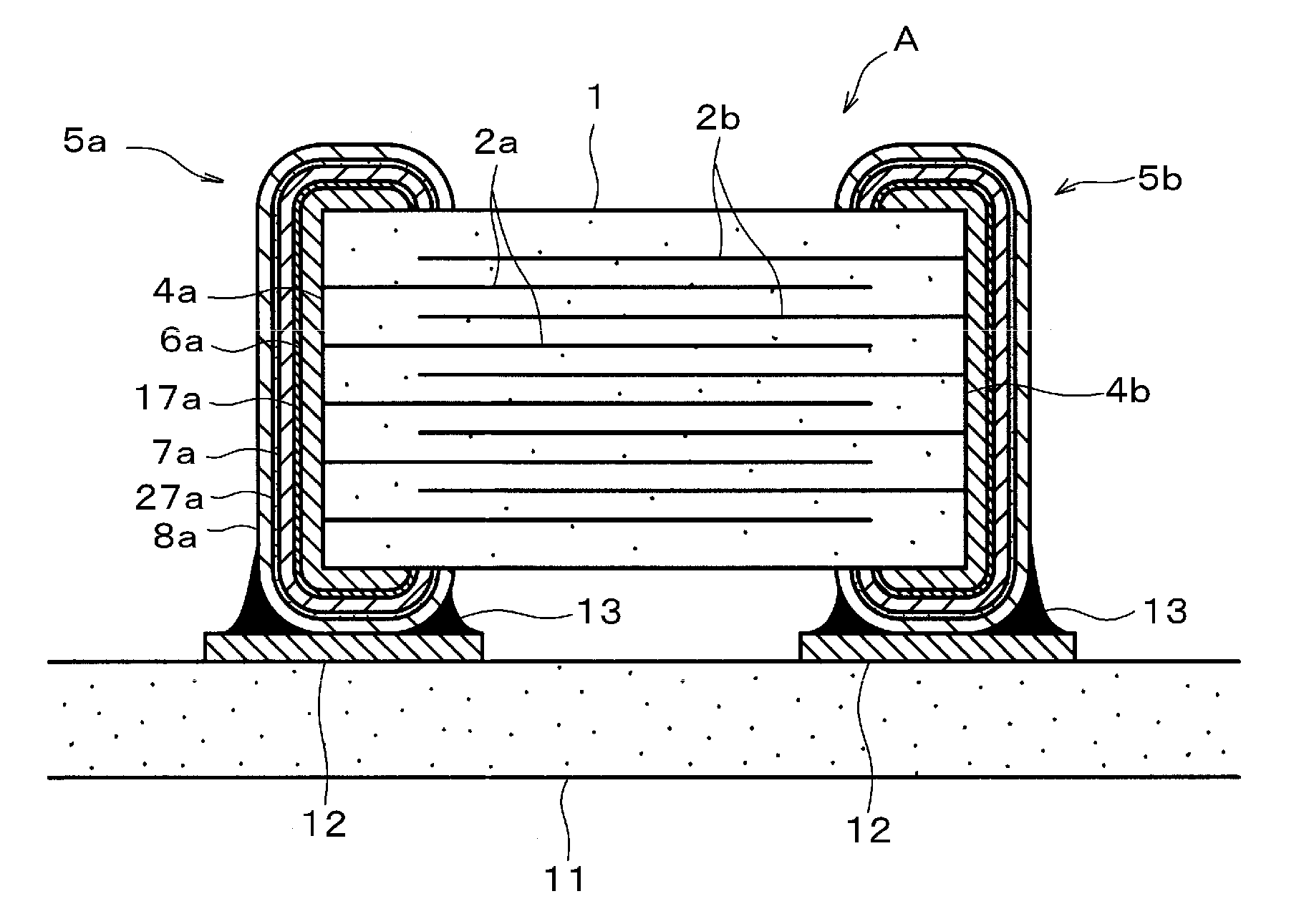
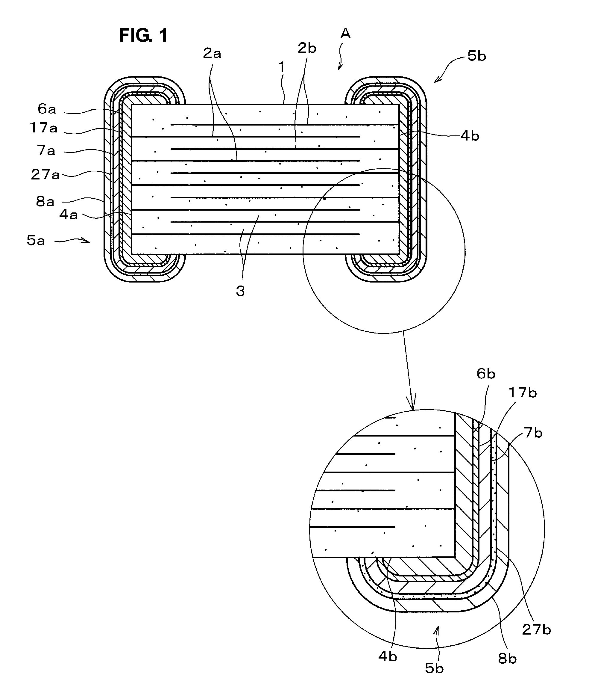
[0046]FIG. 1 is a cross-sectional view of an electronic component (multilayer ceramic capacitor in this EXAMPLE) A produced by a process for producing an electronic component according to an example (EXAMPLE 1) of a preferred embodiment of the present invention.

[0047]As shown in FIG. 1, the multilayer ceramic capacitor A includes a plurality of internal electrodes (Ni electrodes) 2a and 2b alternately disposed; ceramic layers 3, each internal electrode 2a being opposite the corresponding internal electrode 2b with a corresponding one of the ceramic layers 3 provided therebetween; a ceramic body (main body of the electronic component) 1 having end surfaces 4a and 4b, the internal electrodes 2a being connected to the end surface 4a, and the internal electrodes 2b being connected to the end surface 4b; and a pair of external electrodes 5a and 5b, the external electrodes 5a and 5b being disposed on the end surfaces 4a and 4b, respectively, and being connected to the internal electrodes ...

example 2

[0106]In EXAMPLE 2, multilayer ceramic capacitors having the similar structure shown in FIG. 1 as in EXAMPLE 1 were produced in the same production process and the same production conditions as in EXAMPLE 1.

[0107]However, in EXAMPLE 2, conditions for heat-treating the Ni plating layers 7a and 7b disposed on the underlying electrode layers 6a and 6b were as follows. Any other condition was the same as in EXAMPLE 1.

[0108](a) Heat-treatment temperature:

[0109]300° C., 500° C., 700° C., 900° C., and 1100° C.

[0110](b) Oxygen concentration in heat treatment:

[0111]50 ppm, 100 ppm, and 150 ppm

[0112](c) Heat-treatment time:

[0113]1 hour

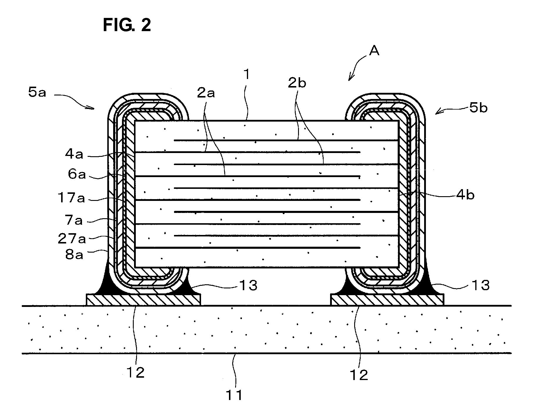
[0114]The resulting multilayer ceramic capacitors were subjected to reflow soldering with lead-free solder containing Zn at about 230° C. in a N2 atmosphere to be mounted on a board. The multilayer ceramic capacitors were left standing for approximately 144 hours at about 125° C., about 1.2 atm, and about 95% RH while a rated voltage was applied, for example. A ...

example 3

[0127]In EXAMPLE 3, multilayer ceramic capacitors having the similar structure shown in FIG. 1 as in EXAMPLE 1 were produced in the same production process and the same production conditions as in EXAMPLE 1.

[0128]However, in EXAMPLE 3, conditions for heat-treating the Ni plating layers disposed on the underlying electrode layers were as follows. Furthermore, the thickness of each Ni plating layer was changed as follows. Other conditions were identical to those in EXAMPLES 1 and 2.

[0129]Heat-Treatment Condition

[0130](a) Heat-treatment temperature:

[0131]600° C.

[0132](b) Oxygen concentration in heat treatment:

[0133]50 ppm

[0134](c) Heat-treatment time:

[0135]0.5 hour, 1 hour, and 2 hours

Thickness of Ni Plating Layer

[0136]0.5 μm, 1.0 μm, 3.0 μm, 5.0 μm, 7.0 μm, and 9.0 μm

[0137]The resulting multilayer ceramic capacitors were subjected to reflow soldering with lead-free solder containing Zn at about 230° C. in a N2 atmosphere to be mounted on a board. The multilayer ceramic capacitors were...


PUM

PropertyMeasurementUnit
thicknessaaaaaaaaaa
particle sizeaaaaaaaaaa

Abstract

A high-reliability electronic component without reduction in insulation resistance under high-temperature and high-humidity conditions has satisfactory solderability of external electrodes. The electronic component includes a main body and external electrodes disposed on surfaces of the main body, the external electrodes include underlying electrode layers each containing a metal, alloy layers each disposed on the corresponding underlying electrode layer, Ni plating layers each disposed on the corresponding alloy layer, Ni oxide layers each disposed on the corresponding Ni plating layers, and upper plating layers each disposed on the corresponding Ni oxide layer, each Ni oxide layer having a thickness of about 150 nm or less, and each Ni plating layer having an average particle size of Ni particles of about 2 μm or more. To form the Ni plating layers having reduced grain boundaries, heat treatment is performed at about 500° C. to about 900° C. inclusive in a reducing atmosphere having an oxygen concentration of about 100 ppm or less.

Description

BACKGROUND OF THE INVENTION[0001]1. Field of the Invention[0002]The present invention relates to an electronic component, a mounting structure of the electronic component, and a process for producing the electronic component. Specifically, the present invention relates to an electronic component having a structure in which external electrodes are disposed on surfaces of the electronic component, a mounting structure of the electronic component, and a process for producing the electronic component.[0003]2. Description of the Related Art[0004]An example of ceramic electronic components each having a structure in which external electrodes are disposed on surfaces of a ceramic element is an electronic chip component, such as a multilayer ceramic capacitor, having a structure including a plurality of internal electrode layers 52a and 52b alternately disposed; ceramic layers 53, each internal electrode layer 52a being disposed opposite the corresponding internal electrode layer 52b with a...

Claims


Application Information

Patent Timeline
Patent Type & Authority Patents(United States)
IPC IPC(8): H05K1/18H01C1/142H01G4/12H01G4/228H01G4/232H01G4/30H01G13/00
CPCH01C1/148H01C7/18H01G4/30H01G4/2325Y10T428/24917H01C1/142H01G4/12
Inventor HORIE, SHIGEYUKIOTA, YUTAKANISHIKAWA, JUN
Owner MURATA MFG CO LTD
Learn More