Method and system for programming, calibrating and driving a light emitting device display

a technology of light-emitting devices and programming methods, applied in the field of display technologies, can solve the problems of slow current-programming of current-driven pixels, non-uniformity of large displays, and inability to provide the accuracy needed for active matrix technology

Active Publication Date: 2009-11-17
IGNIS INNOVATION
View PDF11 Cites 257 Cited by
  • Summary
  • Abstract
  • Description
  • Claims
  • Application Information

AI Technical Summary

Problems solved by technology

However, this technique does not provide the accuracy needed for active matrix, since the active matrix calibration should work for both backplane aging and OLED aging.
Current-programming of current driven pixels is slow due to parasitic line capacitances and suffers from non-uniformity for large displays.
The speed may be an issue when programming with small currents.

Method used


Image

  • Method and system for programming, calibrating and driving a light emitting device display
  • Method and system for programming, calibrating and driving a light emitting device display
  • Method and system for programming, calibrating and driving a light emitting device display

Examples


Embodiment Construction

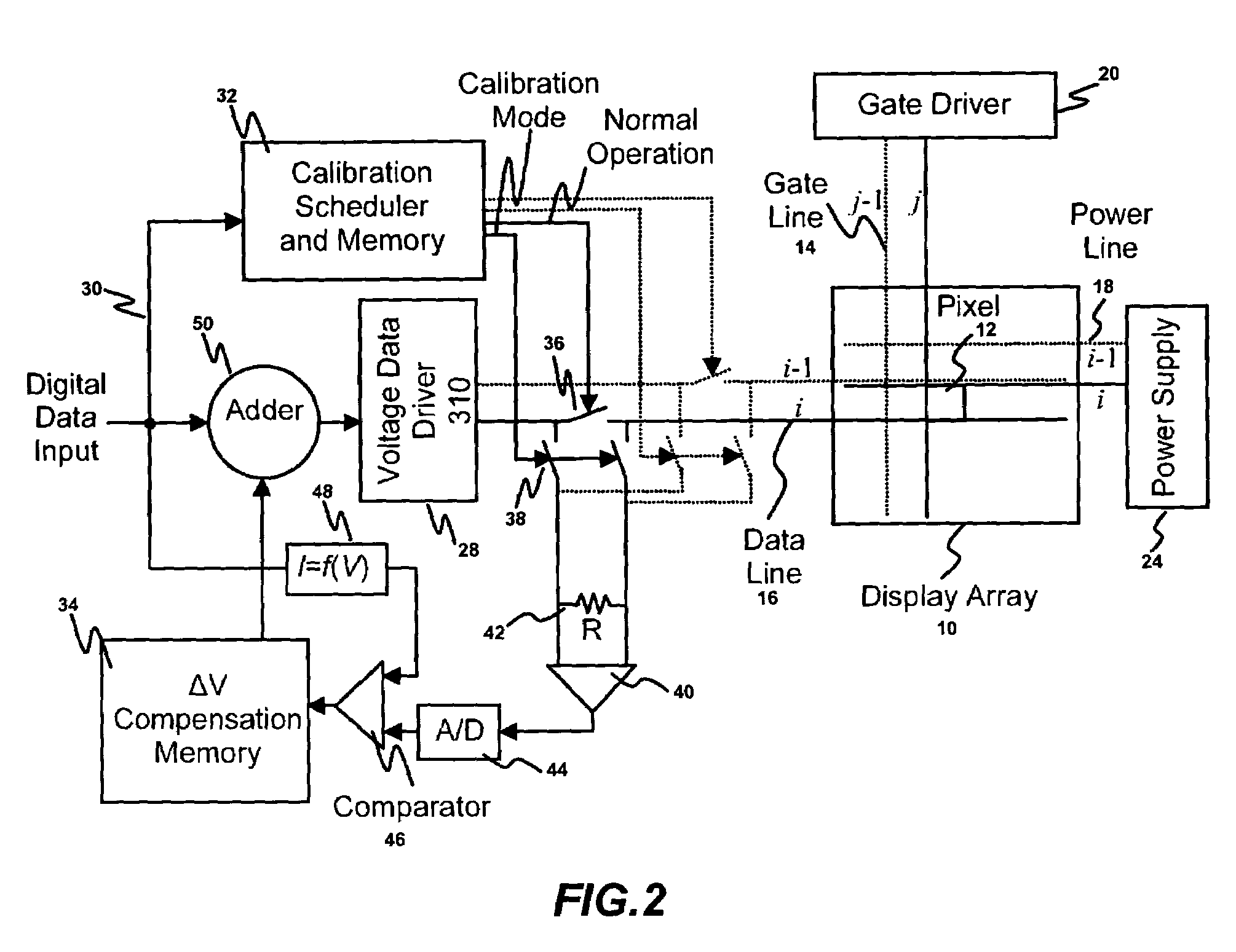
[0044]Embodiments of the present invention are described using a pixel including a light emitting device and a plurality of transistors. The light emitting device may be an organic light emitting diode (OLED). It is noted that “pixel” and “pixel circuit” may be used interchangeably.

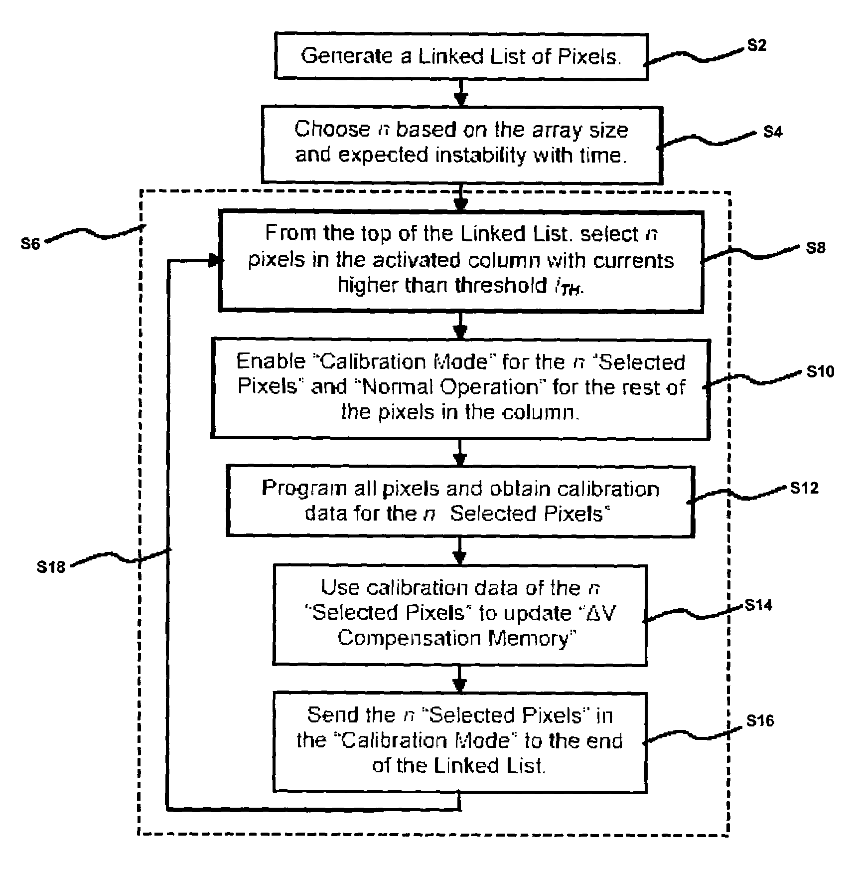
[0045]Real-time calibration-scheduling for a display array having a plurality of pixels is described in detail. FIG. 1 illustrates a process for a calibration-scheduling in accordance with an embodiment of the present invention. According to this technique, the pixels are calibrated based on their aging and / or usage during the normal operation of the display array.

[0046]A linked list of pixels is generated in step S2. The linked list contains an identification of a pixel with high brightness for calibration. The linked list is used to schedule the priority in calibration.

[0047]In step S4, “n” is chosen based on the display size and expected instability with time (e.g. shift in characteristics of transisto...


PUM


Abstract

A method and system for programming, calibrating and driving a light emitting device display is provided. The system may include extracting a time dependent parameter of a pixel for calibration.

Description

FIELD OF INVENTION[0001]The present invention relates to display technologies, more specifically a method and system for programming, calibrating and driving a light emitting device display.BACKGROUND OF THE INVENTION[0002]Recently active-matrix organic light-emitting diode (AMOLED) displays with amorphous silicon (a-Si), poly-silicon, organic, or other driving backplane have become more attractive due to advantages over active matrix liquid crystal displays. For example, the advantages include: with a-Si besides its low temperature fabrication that broadens the use of different substrates and makes feasible flexible displays, its low cost fabrication, high resolution, and a wide viewing angle.[0003]An AMOLED display includes an array of rows and columns of pixels, each having an organic light-emitting diode (OLED) and backplane electronics arranged in the array of rows and columns. Since the OLED is a current driven device, the pixel circuit of the AMOLED should be capable of provi...

Claims


Application Information

Patent Timeline
Patent Type & Authority Patents(United States)
IPC IPC(8): G09G3/32
CPCG09G3/3233G09G3/3241G09G3/3258G09G3/3283G09G3/3291G09G3/006G09G3/3208G09G2300/0842G09G2320/029G09G2320/0295G09G2320/043G09G2320/045G09G2320/0693G09G2310/027G09G3/20G09G3/30G09G3/32H05B33/12G01R19/0092G09G2300/0819G09G2310/0262G09G2320/0285
Inventor NATHAN, AROKIACHAJI, GHOLAMREZA REZASERVATI, PEYMAN
Owner IGNIS INNOVATION
Why Eureka
Try Eureka