Optical-electrical flex interconnect using a flexible waveguide and flexible printed circuit board substrate

a technology of optical-electrical flex interconnection and printed circuit board substrate, which is applied in the direction of optical elements, circuit optical details, instruments, etc., can solve the problems of low-amplitude differential signals, data corruption, video errors,

Active Publication Date: 2009-12-01
NAT SEMICON CORP
View PDF21 Cites 40 Cited by
  • Summary
  • Abstract
  • Description
  • Claims
  • Application Information

AI Technical Summary

Benefits of technology

[0009]A flex interconnect with an integrated electrical-to optical and optical-to-electrical transport layer, which enables the optical transport of critical high speed data without the need of expensive and bulky optical connectors, is disclosed. The flex interconnect assembly includes a flexible printed circuit substrate, which includes one or more electrical interconnects, formed on the flexible printed circuit substrate, for transmitting one or more electrical signals respectively. The flexible printed circuit substrate also includes an optical waveguide mounted onto the substrate. The optical waveguide includes an integral optical transport layer, including electrical-to-optical and optical-to-electrical interfaces connected at either end of the optical waveguide. With the integrated optical transport layer, the flex interconnect can receive electrical signals, convert and transmit them to optical signals, and then convert them back to electrical signals, all without expensive and bulky opto-electrical connectors. In one embodiment, the flex interconnect is used for transmitting both electrical and optical signals in a portable device, such as a cell phone, PDA, personal computer, and the like.

Problems solved by technology

Low amplitude differential signals, however, are susceptible to data corruption when exposed to RF noise.
This is particularly troublesome in wireless portable devices.
If the portable device is streaming video while transmitting or receiving radio signals, the RF noise may corrupt the low amplitude signals, resulting in video errors.

Method used


Image

  • Optical-electrical flex interconnect using a flexible waveguide and flexible printed circuit board substrate
  • Optical-electrical flex interconnect using a flexible waveguide and flexible printed circuit board substrate
  • Optical-electrical flex interconnect using a flexible waveguide and flexible printed circuit board substrate

Examples


Embodiment Construction

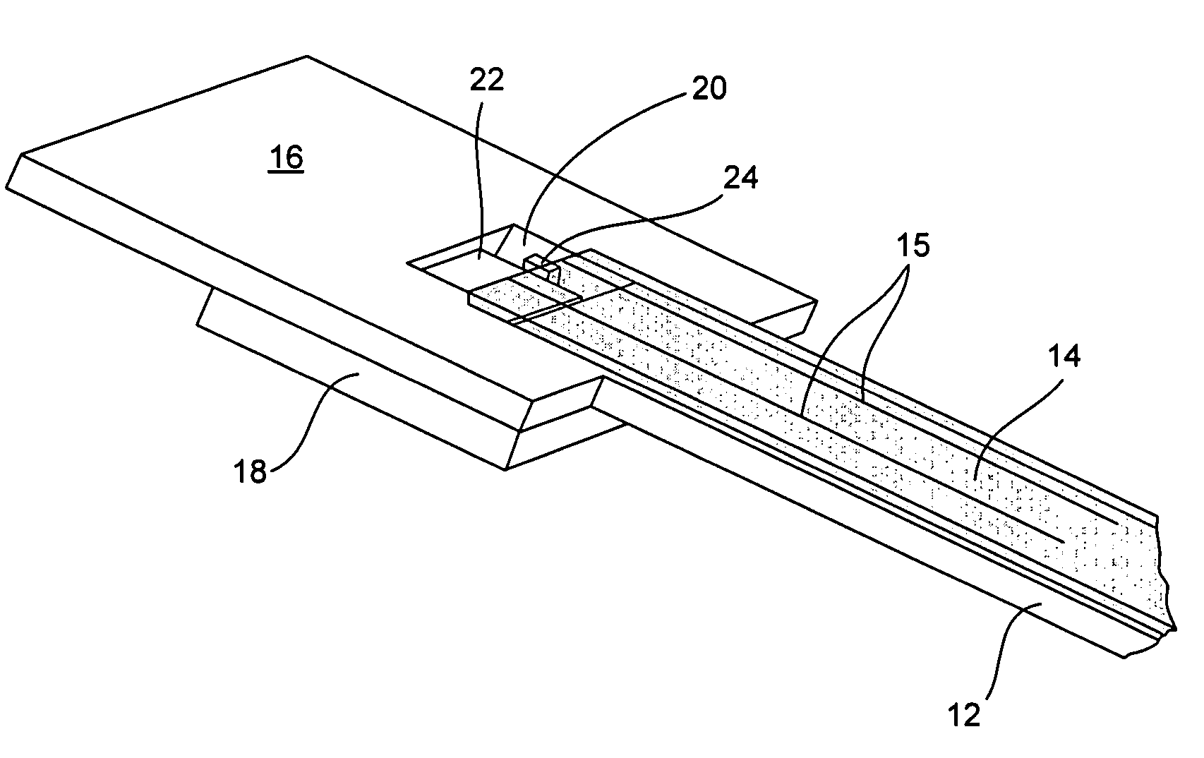
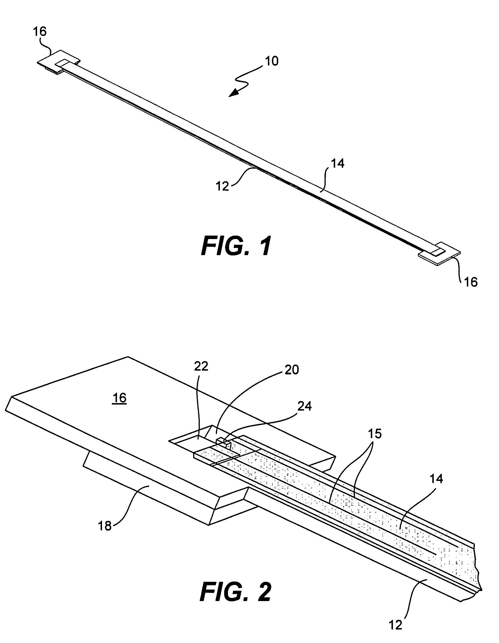
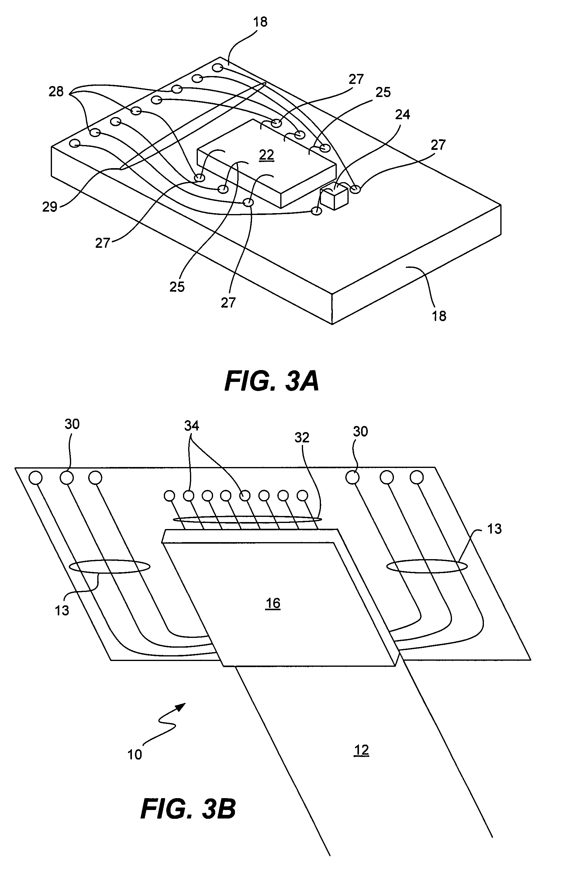
[0021]Referring to FIG. 1, a perspective view of an opto-electric flex interconnect assembly according to the present invention is shown. The opto-electric flex interconnect assembly 10 includes a flexible printed circuit substrate 12 with one or more electrical interconnects 13 (not visible) for transmitting electrical signals and a flexible optical waveguide 14 mounted onto the substrate 12. The optical waveguide 14 includes one or more cores 15 (also not visible) for transmitting optical signals. In one embodiment, the electrical interconnects are used for transmitting power and control signals, whereas the optical cores are used for transmitting data signals.

[0022]The assembly 10 further includes electrical-to-optical and optical-to-electrical interfaces 16 located at either end of the assembly 10. As described in more detail below, the waveguide 14 and interfaces 16 provide an optical transport layer integrated within the assembly 10. With interfaces 16, expensive and bulky opt...


PUM


Abstract

A flex interconnect with an integrated electrical-to optical and optical-to-electrical transport layer, which enables the optical transport of critical high speed data without the need of expensive and bulky optical connectors. The flex interconnect assembly includes a flexible printed circuit substrate, which includes one or more electrical interconnects, formed on the flexible printed circuit substrate, for transmitting one or more electrical signals respectively. The flexible printed circuit substrate also includes an optical waveguide mounted onto the substrate. The optical waveguide includes an integral optical transport layer, including electrical-to-optical and optical-to-electrical interfaces connected at either end of the optical waveguide. With the integrated optical transport layer, the flex interconnect can receive electrical signals, convert and transmit them to optical signals, and then convert them back to electrical signals, all without expensive and bulky opto-electrical connectors. In one embodiment, the flex interconnect is used for transmitting both electrical and optical signals in a portable device, such as a cell phone, PDA, personal computer, and the like.

Description

BACKGROUND OF THE INVENTION[0001]1. Field of the Invention[0002]The present invention relates generally to flex interconnects, and more particularly, to a flex interconnect including a optical waveguide formed on a flexible printed circuit board substrate for transmitting and receiving both optical and electrical signals.[0003]2. Description of the Related Art[0004]The functionality provided on portable devices, such as laptop computers, cell phones, personal-digital assistants (PDAs), cameras, and MP3 players, is both converging and continually increasing. For example, not that long ago, a person typically had a separate laptop computer for performing data processing, sending emails and text messaging, a cell phone for making wireless phone calls, a camera for taking pictures, and an MP3 player for listening to music and other audio content. More recently, however, the functionality provided by one or more of these separate devices has been implemented all on one device. For exampl...

Claims


Application Information

Patent Timeline
Patent Type & Authority Patents(United States)
IPC IPC(8): G02B6/12G02B6/10
CPCG02B6/1221H05K1/0274H05K1/0393G02B6/4214
Inventor DEANE, PETER
Owner NAT SEMICON CORP
Why Eureka
Try Eureka