Semiconductor device module structure

a technology of semiconductor devices and modules, applied in semiconductor devices, semiconductor/solid-state device details, electrical apparatus, etc., can solve the problems of joule heat generation, cell damage, cell top face side of semiconductor elements not cooling, etc., to reduce stress arising in the guard ring part, reduce the effect of voltage withstandability and prevent cell damag

Inactive Publication Date: 2010-02-16
HONDA MOTOR CO LTD
View PDF9 Cites 0 Cited by
  • Summary
  • Abstract
  • Description
  • Claims
  • Application Information

AI Technical Summary

Benefits of technology

[0024]By this means, it is possible to reduce stresses arising in the guard ring part and make voltage withstandability drop and cell breakdown unlikely to occur. That is, with this invention, it becomes possible to prevent cell breakdown caused by a strap doubling as a lead and a heat-sinking plate being mounted on the upper face side of a power semiconductor element and voltage withstandability drop caused by stresses acting on the guard ring part.
[0025]In the invention, preferably, the module structure of the semiconductor device further has a diode part, and a cathode electrode above the diode part and the upper heat-sinking part are connected. By this means it is possible to reduce stresses arising in the guard ring part and form a semiconductor device in which voltage withstandability drop and cell breakdown and element breakdown do not readily occur.

Problems solved by technology

However, it has sometimes happened that the cells on the top face side of the semiconductor element are not cooled and cells are destroyed.
When cells operate in this kind of state, current flows, joule heat is produced, and a latchup phenomenon tends to occur.
When latchup occurs, locally current flows and high heat is produced, and this has been a cause of cell breakdown such as PN junction breakdown.
Due to this cracking, as a result a voltage withstandability drop is brought about.

Method used


Image

  • Semiconductor device module structure
  • Semiconductor device module structure
  • Semiconductor device module structure

Examples


first embodiment

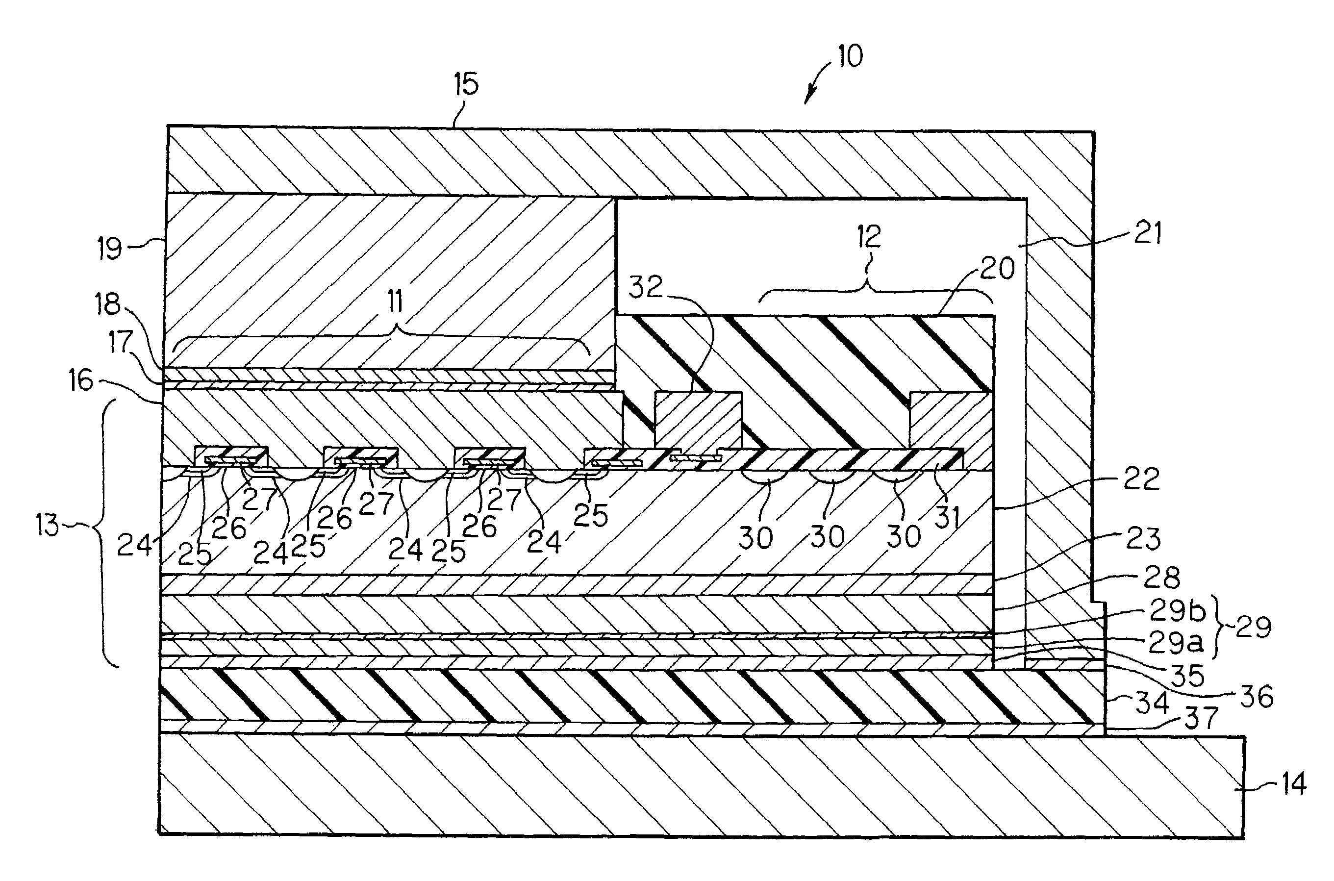
[0033]FIG. 1 is a sectional view showing a main part of a module structure of a semiconductor device according to the invention. In this embodiment an insulated gate bipolar transistor (IGBT) is used as the semiconductor device. An IGBT module 10 has heat-sinking plates 14, 15 for cooling a semiconductor element 13 having a working part 11 and a guard ring part 12.

[0034]The heat-sinking plates 14, 15 are made up of a lower heat-sinking plate 14 joined to a substrate 34 made of an insulator provided below the working part 11 and the guard ring part 12, and an upper heat-sinking plate (strap) 15 having a part joined to an emitter electrode 16 at the upper part of the working part 11 via a metal 17, a metal 18 and an adhesive 19 and a part having a gap 21 provided between itself and a passivation film 20 deposited on the upper part of the guard ring part 12 and not joined thereto.

[0035]The metal 17 and the metal 18 are correlated metals of the emitter electrode 16 and the adhesive 19. ...

second embodiment

[0047]FIG. 3 is a sectional view showing a module structure of a semiconductor device according to a In this embodiment, a semiconductor element constituting the semiconductor device is a diode. A diode module 40 has heat-sinking plates 44, 45 for cooling a semiconductor element 43 having a working part 41 and a guard ring part 42.

[0048]The heat-sinking plates 44, 45 consist of a lower heat-sinking plate 44 joined to a substrate 58 made of an insulator provided below the working part 41 and the guard ring part 42, and an upper heat-sinking plate (strap) 45 having a part joined to a cathode electrode 46 at the top of the working part 41 by way of a metal 47, a metal 48 and an adhesive 49, and a part having a gap 51 provided between itself and a passivation film 50 deposited on the upper part of the guard ring part 42 and not joined thereto.

[0049]The metal 47 and the metal 48 are correlated metals of the cathode electrode 46 and the adhesive 49. The metal 47 is silver (Ag) or gold (A...

third embodiment

[0061]To explain briefly, the semiconductor device module 60 of the third embodiment has heat-sinking plates 61, 62 for cooling a semiconductor element (IGBT element) 13 and a semiconductor element (diode element) 43. The heat-sinking plates 61, 62 consist of a lower heat-sinking plate 61 provided below the semiconductor elements 13, 43 and an upper heat-sinking plate 62 having parts joined to the electrodes 16, 46 at the tops of the working parts 11, 41 and parts not joined to the passivation films 20, 50 deposited on the guard ring parts 12, 42.

[0062]The semiconductor device module 60 is joined to a radiator such as a heat sink below the lower heat-sinking plate 61 with a highly thermally conductive grease or the like. Heat produced in the IGBT element 13 and the diode element 43 when the diode module 60 is operating is conducted to the radiator through the lower heat-sinking plate 61 and the upper heat-sinking plate 62 and radiated away. By this means the IGBT element 13 and the ...


PUM


Abstract

A semiconductor module includes: a semiconductor element (13) having a working unit (11) and a guard ring unit (12); and heat radiation members (15, 14) arranged on an upper surface and a lower surface of the semiconductor element for cooling the semiconductor element. A passivation film (20) covers the guard ring but does not cover the working unit. The upper heat radiation member (15) is made of a flat metal plate connected to the working unit without contact with the passivation film. The upper heat radiation member is connected to the lower heat radiation member (14) in the thermo-conducting way.

Description

TECHNICAL FIELD[0001]The present invention relates to a module structure of a semiconductor device and, more particularly, to a module structure of a semiconductor device having a heat-sinking mechanism on a device upper part in a semiconductor device including a power device such as an insulated gate bipolar transistor (IGBT).BACKGROUND ART[0002]As switching semiconductor elements for controlling relatively large currents, power devices are known. Power devices include power transistors and power MOSFETs and IGBTs and the like. Of these, IGBTs are used for example in inverters of electric vehicles as devices having the merits of ease of driving resulting from voltage drive and low loss resulting from conductivity modulating effect.[0003]FIG. 5 shows the structure of a conventional IGBT module. This IGBT module 100 has a heat-sinking plate 104 for cooling a semiconductor element 103 having a working part 101 and a guard ring part 102. The heat-sinking plate 104 consists of a bottom ...

Claims


Application Information

Patent Timeline
Patent Type & Authority Patents(United States)
IPC IPC(8): H01L23/52H01L23/34H01L23/48H01L23/051H01L23/31H01L23/373H01L23/58H01L27/04H01L29/06H01L29/739H01L29/78H01L29/861
CPCH01L23/051H01L23/3171H01L23/3735H01L23/585H01L25/072H01L29/7395H01L29/7397H01L29/7811H01L29/7813H01L29/8611H01L2924/1305H01L2224/73265H01L24/48H01L29/0619H01L29/402H01L2224/48091H01L2924/01079H01L2924/13055H01L2924/13091H01L2924/00014H01L2924/00H01L2224/451H01L2224/45124H01L2924/12036H01L2224/40H01L24/45H01L2224/02166H01L2924/00015H01L2224/45015H01L2924/207H01L2224/37099
Inventor KITAMURA, KENJIYATAKA, SHINICHIENDO, TAKAOTOMINAGA, YUUJIROTANAKA, TOSHIHIDESATO, KOICHIRO
Owner HONDA MOTOR CO LTD
Why Eureka
Try Eureka