
Defect classification using a logical equation for high stage classification

a logical equation and high-stage classification technology, applied in the field of defect classification methods, can solve the problems of difficult to achieve a high yield for semiconductor manufacturing, automatic classification cannot be appropriately done, and the post-processing manufacturing process of semiconductors is more complicated than ever, so as to achieve better classification performance and better classification performance

Active Publication Date: 2010-07-13
HITACHI HIGH-TECH CORP
View PDF13 Cites 10 Cited by
  • Summary
  • Abstract
  • Description
  • Claims
  • Application Information

AI Technical Summary

Benefits of technology

The present invention relates to a method for automatically classifying defects based on their appearance. The method includes steps for calculating classification criteria based on a plurality of training defect groups, classifying a defect cluster based on its true classification class, calculating the accuracy ratio of the classification criteria based on the difference between the classification result and the true classification class, and estimating the classification accuracy ratio based on the relationship between the number of training defects and the classification accuracy ratio. The invention also provides a resetting technique for the classification criteria to ensure better classification performance. The technical effects of the invention include improved accuracy in defect classification and a more reliable basis for automatic defect classification.

Problems solved by technology

As semiconductors getting finer in structure, the semiconductor post-processing manufacturing process has become more complicated than ever.
With the conventional process control based on the changing number of semiconductor defects detected by outer appearance inspection of semiconductor wafers, it is getting difficult to achieve a high yield for semiconductor manufacturing.
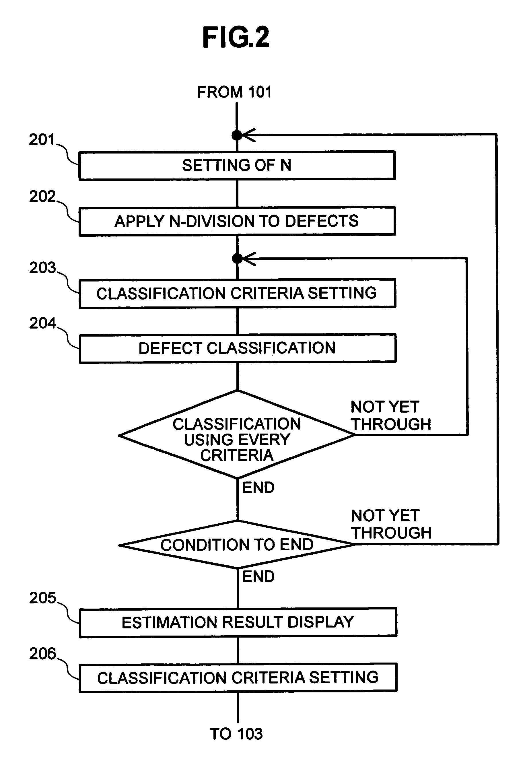
Thus, the problem of the conventional technology is that the defect feature distribution may look different once automatic classification is started, and if so, automatic classification cannot be appropriately done.
Thus, automatic classification cannot be normally done if no measure is taken therefor.
Therefore, it is difficult to determine whether the classification criteria set at this point of time is good enough or not.
The problem here is that, however, always monitoring defect classification requires a lot of efforts after once automatic classification is started.
Thus, there is no more point for automatic classification, and such an operation cannot be practically carried out in the actual manufacturing lines.
The issue here is that the recent process control requires defect classification in a detailed manner, and to make it a reality, the number of dimensions in the feature amount space is getting increased.
Therefore, it is difficult to automatically detect the change of the feature amount distribution because the defect distribution is initially derived from the small number of samples.
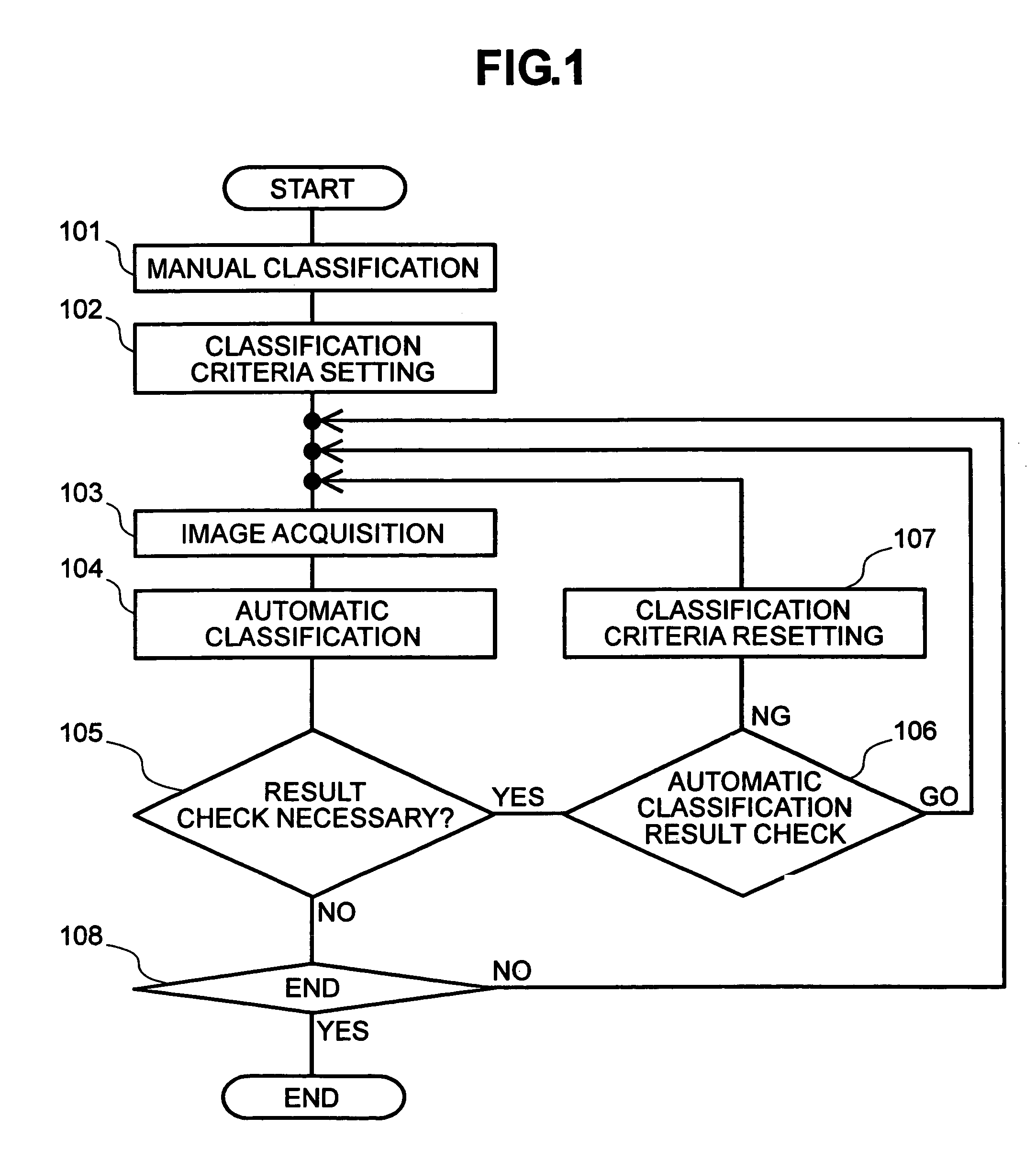
Further, even if the classification criteria is determined as having a problem in its setting through defect monitoring after automatic classification is started, actually, the classification criteria has been considerably difficult to appropriately reset.
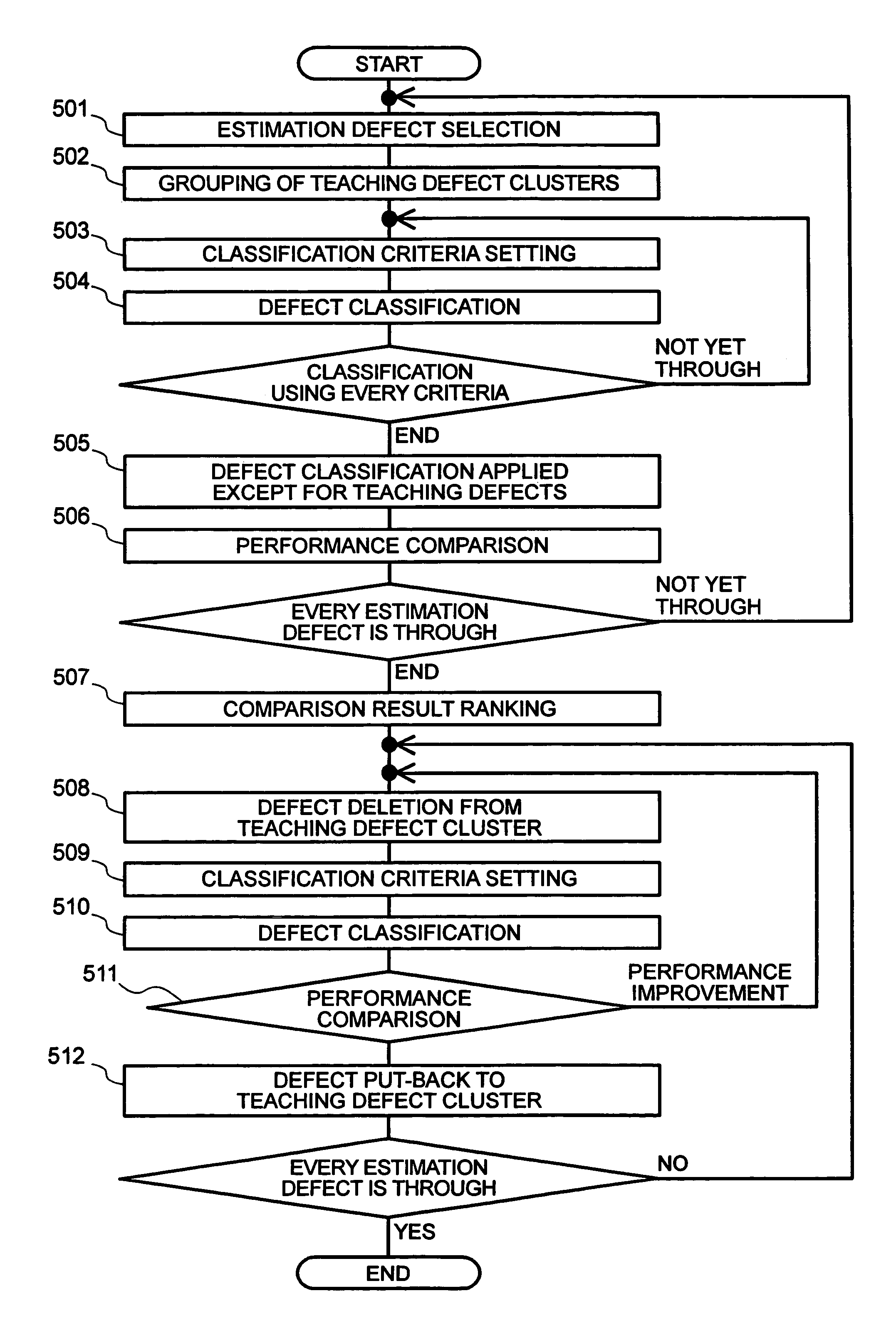
The reason is that it is generally impossible to guarantee whether resetting of the classification criteria leads to the classification result more accurate than the one as a result of defect processing in volume following the setting of classification criteria.
Moreover, resetting of the classification criteria causes the classification result to differ between before and after the resetting.
This resultantly varies the number of defects on a classification class basis before and after the resetting, thereby causing inconvenience for process control.
However, if every defect is subjected to feature amount extraction, the performance will be resultantly lowered especially if some defects are added later.
However, it is still difficult for the general users to know selecting which defect leads to the best result.
As such, resetting of the classification criteria hardly leads to the better performance.

Method used


Image

  • Defect classification using a logical equation for high stage classification
  • Defect classification using a logical equation for high stage classification
  • Defect classification using a logical equation for high stage classification

Examples


Embodiment Construction

[0021]In the below, an embodiment of the present invention is described by referring to FIGS. 1 to 8.

[0022]As to a semiconductor wafer, the pattern of which is formed to be of multilayer structure by going through a plurality of steps. In the process for manufacturing such a multilayer structure, for monitoring the manufacturing process, every layer is subjected to outer appearance inspection, and if any defect is detected thereby, the defect is reviewed and then classified according to defect type. For defect reviewing, various manners have been proposed and put into practical use as follows:

[0023]1. the manner of reviewing images picked up by an inspection device during inspection,

[0024]2. the revisit manner of picking up any defect images again using an outer appearance image pickup unit of the inspection device,

[0025]3. the manner of performing a review using a review device such as a review Scanning Electronic Microscope (SEM) of a type different from the inspection device.

[002...


PUM


Abstract

With little efforts, to estimate the appropriateness of automatic defect classification, and to make classification criteria settable with a guarantee for the better classification performance, defects unknown with their classification classes are classified based on two different classification criteria. Also, defects differed in classification results are collected, and each thereto, a defect classification class is provided by using a manual. Then, the defects provided with the classification classes are divided into two types of groups: one is a setting group for the classification criteria; and the other is an evaluation group. Based on the classification criteria that is so set as to classify the defects included in the setting group with the maximum performance, the classification performance of a case where classification is applied to defects included in the evaluation group is calculated, and the appropriateness of thus set classification criteria is evaluated.

Description

BACKGROUND OF THE INVENTION[0001]The present invention relates to a defect classification method applied to industrial products utilizing a thin film technology and, more specifically, to a method for automatically setting classification criteria for semiconductor products with which detailed defect review and classification are considered important after defect detection through post-step inspection in the automatic defect classification method.[0002]As semiconductors getting finer in structure, the semiconductor post-processing manufacturing process has become more complicated than ever. With the conventional process control based on the changing number of semiconductor defects detected by outer appearance inspection of semiconductor wafers, it is getting difficult to achieve a high yield for semiconductor manufacturing. In consideration thereof, proposed is Automatic Defect Classification (ADC) for automatically classifying any defects through analysis of images derived after ins...

Claims


Application Information

Patent Timeline
Patent Type & Authority Patents(United States)
IPC IPC(8): G06K9/00G06K9/62G06T7/00
CPCG06T7/0004G06T2207/30148
Inventor HONDA, TOSHIFUMIMIYAMOTO, ATSUSHIOKUDA, HIROHITO
Owner HITACHI HIGH-TECH CORP
Learn More