Methods for reading a pixel and for writing to a pixel and a device having pixel reading capabilities and pixel writing capabilities

Inactive Publication Date: 2010-09-07
PIXIM ISRAEL
View PDF4 Cites 15 Cited by
  • Summary
  • Abstract
  • Description
  • Claims
  • Application Information

AI Technical Summary

Benefits of technology

[0007]A device having pixel reading capabilities, the device includes a pixel, a control circuit and a readout circuit connected to the pixel and to the control circuit; wherein the pixel includes a photo-detector, an input transistor, a second, third and fourth transistor; wherein the photo-detector and the input transistor are connected to a first node; wherein the input transistor, second and fourth transistors are connected to a second node; wherein the third transistor outputs a pixel output signal and is connected to the fourth transistor; and wherein the first, second and th

Problems solved by technology

The performance of CMOS pixels is limited by their thermal noise.
When this reset phase

Method used


Image

  • Methods for reading a pixel and for writing to a pixel and a device having pixel reading capabilities and pixel writing capabilities
  • Methods for reading a pixel and for writing to a pixel and a device having pixel reading capabilities and pixel writing capabilities
  • Methods for reading a pixel and for writing to a pixel and a device having pixel reading capabilities and pixel writing capabilities

Examples


Example

DETAILED DESCRIPTION OF THE DRAWINGS

[0038]In the context of the present patent application and the claims “active” and “conductive” are assumed to be equivalent terms. In the context of the present patent application and the claims “inactive” and “non-conductive” are assumed to be equivalent terms. In the context of the present patent application and the claims “weak conductive” and “sub threshold” and “weak inversion” are assumed to be equivalent terms.

[0039]It is noted that the term “capacitance” can describe a parasitic capacitance, a non-parasitic capacitor or a combination thereof. A capacitance can be defined within a single pixel or can be defined between one pixel to the other, between one pixel to a wire, between one wire to another, and the like.

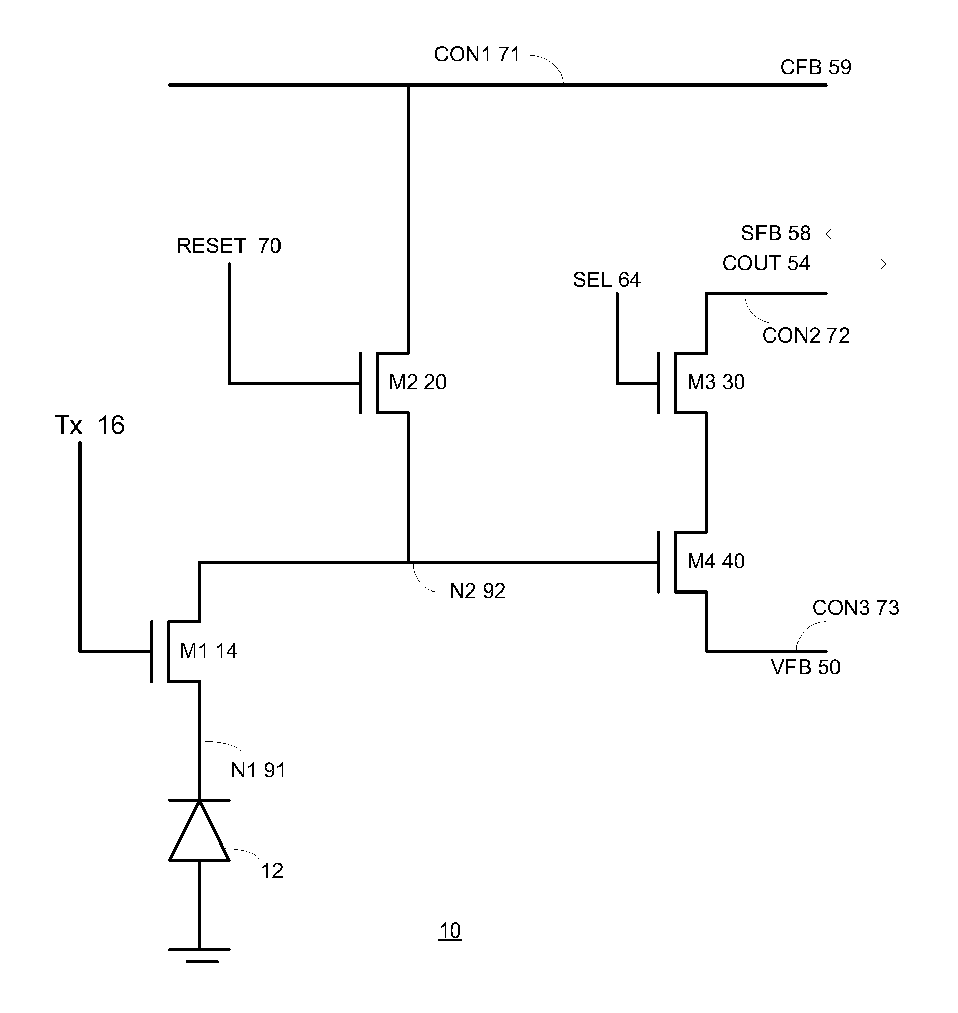
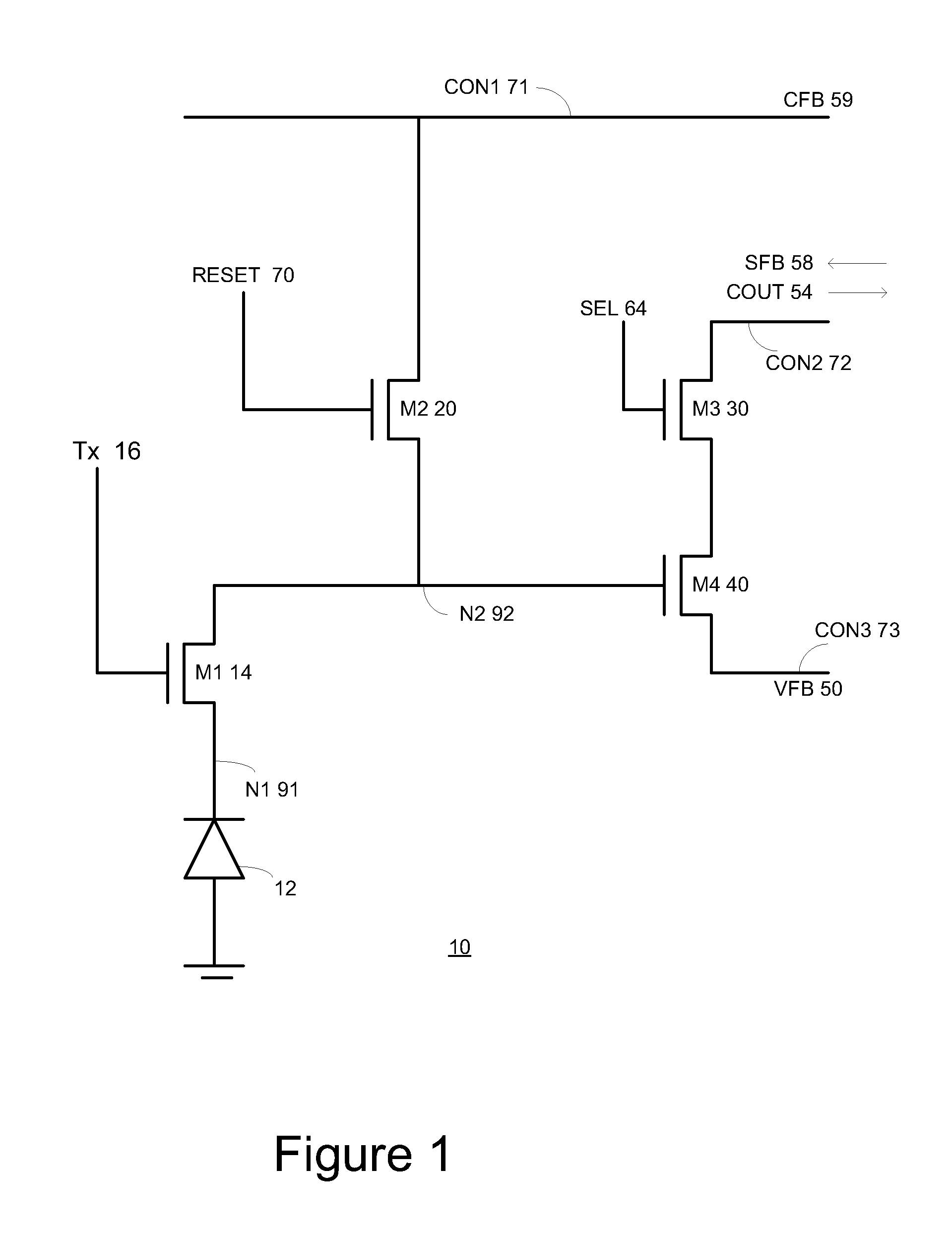
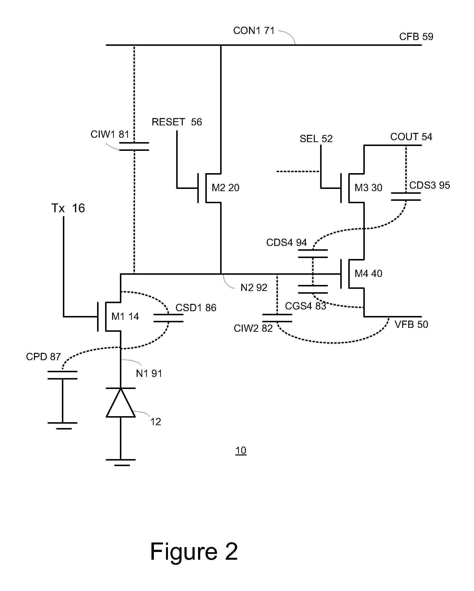
[0040]FIG. 1 illustrates pixel 10 according to an embodiment of the invention.

[0041]Pixel 10 includes photo-detector 12, input transistor 14, second transistor 20, third transistor 30 and fourth transistor 40. For simplicity of exp...


PUM


Abstract

Methods for reading a pixel and writing to a pixel and devices having pixel reading capabilities and pixel writing capabilities. A method for reading a pixel includes: activating a second transistor that is coupled to a second node while maintaining an input transistor inactive; wherein the first transistor is coupled between the second node and a photo-detector; inactivating the second transistor; compensating for second node voltage change resulting from the inactivating of the second transistor by providing a feedback signal via at least one capacitance that capacitively couples the pixel node to the second node; and activating the input transistor and measuring a pixel output signal.

Description

RELATED APPLICATIONS[0001]This application claims priority of U.S. provisional patent Ser. No. 60 / 807,848 filing date Jul. 20, 2006.FIELD OF THE INVENTION[0002]The invention relates to methods for reading a pixel and for writing to a pixel and to devices having pixel reading capabilities and / or pixel writing capabilities.BACKGROUND OF THE INVENTION[0003]Digital cameras include a two-dimensional photo-detector array. A single pixel can include one or more photo-detectors as well as multiple transistors. Typical photo-detectors include photodiodes, phototransistors, photo-gates, hole accumulation diodes, pinned diodes, avalanche diodes, buried accumulation and transfer layer devices.[0004]The performance of CMOS pixels is limited by their thermal noise. This noise is also known as reset noise of KTC noise. During a reset phase of the pixel a reset voltage is provided to the pixel and especially to a reset transistor of the pixel. When this reset phase ends the reset transistor enters ...

Claims


Application Information

Patent Timeline
IPC IPC(8): H04N3/14H04N5/335H01L27/00H01L27/14H04N5/363H04N5/3745
CPCH04N5/363H04N5/3741H04N5/37457H04N25/65H04N25/766H04N25/778H04N25/60H04N25/76
Inventor KOIFMAN, VLADIMIR
Owner PIXIM ISRAEL
Why Eureka
Try Eureka