Phase-change memory device having phase change material pattern shared between adjacent cells and electronic product including the phase-change memory

a memory device and phase-change technology, applied in semiconductor devices, digital storage, instruments, etc., can solve the problems of easy damage to phase-change material patterns, and achieve the effect of reducing electric interferen

Active Publication Date: 2010-09-21
SAMSUNG ELECTRONICS CO LTD
View PDF7 Cites 35 Cited by
  • Summary
  • Abstract
  • Description
  • Claims
  • Application Information

AI Technical Summary

Benefits of technology

[0007]The present invention provides a phase-change memory device including a phase-change material pattern that can be formed with less damaged portions and reduce electric interference between neighboring memory cells, and an electronic product including the phase-change memory device.

Problems solved by technology

During the patterning process, the phase-change material pattern can be damaged.
Particularly, when the phase-change material pattern includes separate islands for respective cells, the phase-change material pattern can be easily damaged since four sides of each island are exposed.

Method used


Image

  • Phase-change memory device having phase change material pattern shared between adjacent cells and electronic product including the phase-change memory
  • Phase-change memory device having phase change material pattern shared between adjacent cells and electronic product including the phase-change memory
  • Phase-change memory device having phase change material pattern shared between adjacent cells and electronic product including the phase-change memory

Examples


Embodiment Construction

[0027]The present invention will now be described more fully with reference to the accompanying drawings, in which exemplary embodiments of the invention are shown. The invention may, however, be embodied in many different forms and should not be construed as being limited to the embodiments set forth herein; rather, these embodiments are provided so that this disclosure will be thorough and complete, and will fully convey the concept of the invention to those skilled in the art. In the drawings, the thicknesses of layers and regions are exaggerated for clarity, and like reference numerals denote like elements.

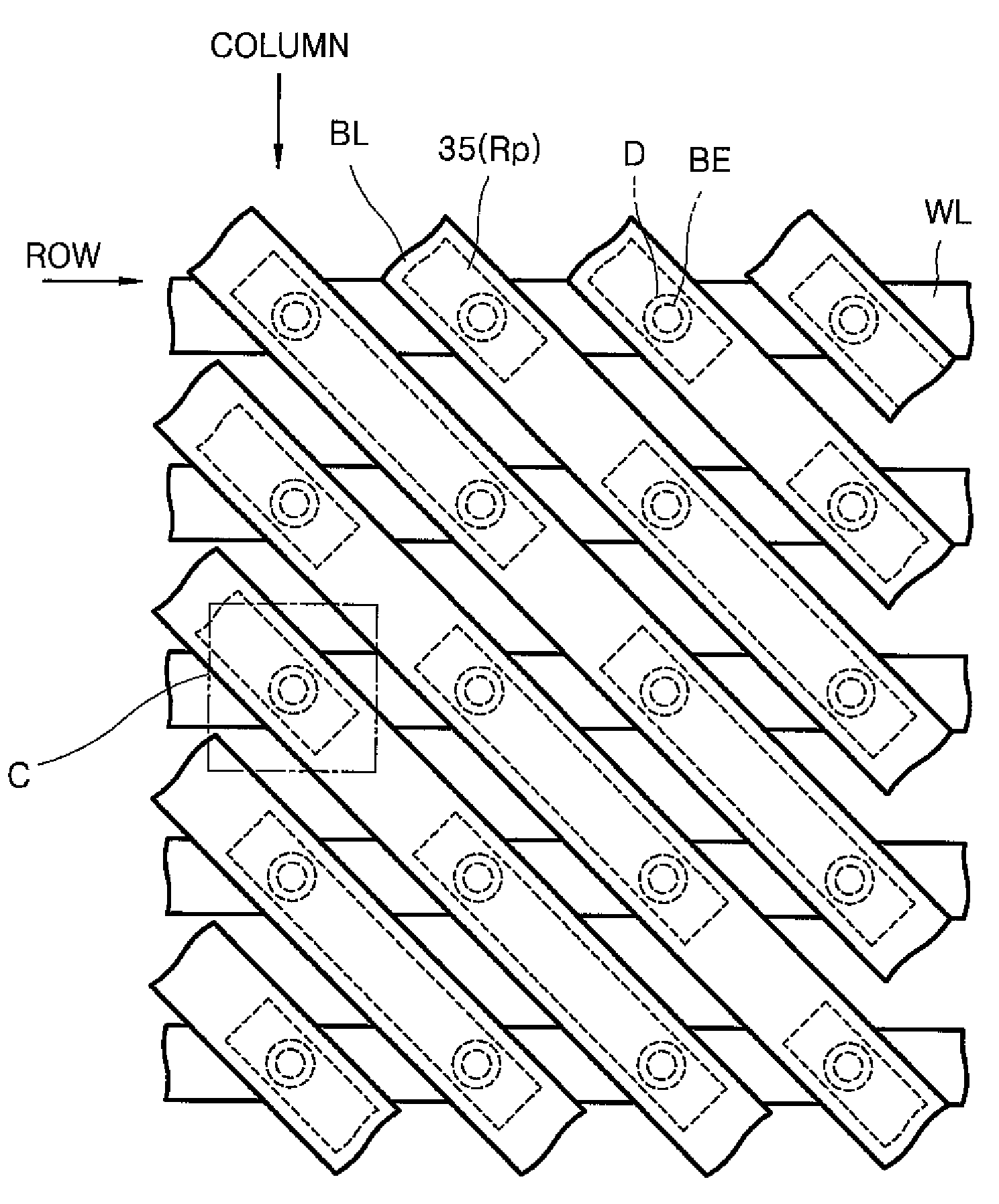
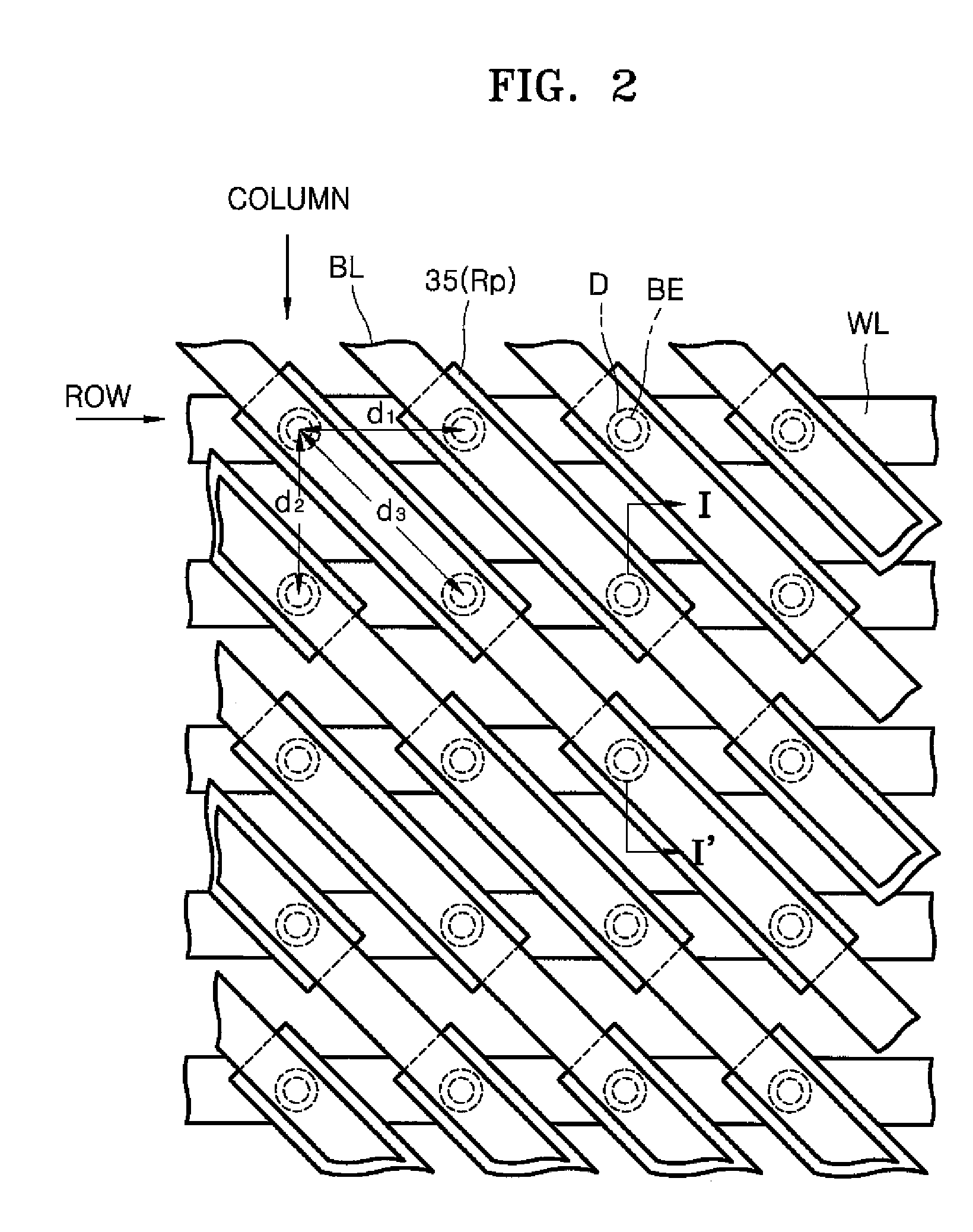
[0028]FIG. 1 is an equivalent circuit diagram illustrating a part of a cell array region of a phase-change memory device according to an embodiment of the present invention.

[0029]Referring to FIG. 1, the cell array region of the phase-change memory device includes a plurality of first signal lines (word lines WL) and a plurality of second signal lines (bit lines BL) crossing w...


PUM


Abstract

Provided is a phase-change memory device including a phase-change material pattern of which strips are shared by neighboring cells. The phase-change memory device includes a plurality of bottom electrodes arranged in a matrix array. The phase-change material pattern is formed on the bottom electrodes, and the strips of the phase-change material pattern are electrically connected to the bottom electrodes. Each strip of the phase-change material pattern is connected to at least two diagonally neighboring bottom electrodes of the bottom electrodes.

Description

CROSS-REFERENCE TO RELATED PATENT APPLICATION[0001]This application claims the benefit of Korean Patent Application No. 10-2006-0134177, filed on Dec. 26, 2006, in the Korean Intellectual Property Office, the disclosure of which is incorporated herein in its entirety by reference.BACKGROUND OF THE INVENTION[0002]1. Field of the Invention[0003]The present invention relates generally to a semiconductor memory device, and more particularly, but without limitation, to a phase-change memory device including a phase-change material pattern shared between adjacent cells.[0004]2. Description of the Related Art[0005]A phase-change memory device is a nonvolatile memory device using a phase-change material of which resistance varies according to the phase of the phase-change material. Each cell of a phase-change memory device includes a switching unit and a phase-change resistor electrically connected to the switching unit. The phase-change resistor includes a phase-change material pattern.[00...

Claims


Application Information

Patent Timeline
Patent Type & Authority Patents(United States)
IPC IPC(8): H01L47/00
CPCG11C11/5678G11C13/0004H01L27/2409H01L27/2436H01L27/2472H01L45/06H01L45/1233H01L45/144H01L45/1675H10B63/82H10B63/20H10B63/30H10N70/231H10N70/8828H10N70/063H10N70/826
Inventor AN, HYEONG-GEUNHORII, HIDEKISHIN, JONG-CHANAHN, DONG-HOBAE, JUN-SOO
Owner SAMSUNG ELECTRONICS CO LTD
Why Eureka
Try Eureka