Voltage increase circuit for elevated voltage charge

A technology for boosting capacitors and charges, which is applied in the direction of conversion equipment without intermediate conversion to AC, and can solve problems such as system damage, cost rise, and increased production costs.

Inactive Publication Date: 2008-02-20
G TIME ELECTRONICS
View PDF1 Cites 4 Cited by
  • Summary
  • Abstract
  • Description
  • Claims
  • Application Information

AI Technical Summary

Problems solved by technology

However, at the same time, the characteristics of the above-mentioned depletion-type metal-oxide-semiconductor transistors also make the improved charge boosting circuit 200 switch over the working clock. After the voltage of node A has been boosted, the depletion-type N-channel The metal-oxide-semiconductor transistor still cannot be turned off (turn off), so a reverse leakage current Iq is generated along a path 210, and the reverse leakage current Iq and the charge boosting circuit 100 adopt enhancement-type N-channel transistors (Enhancement-type N-channel transistors). Transistor) the critical voltage Vt of the supercharging effect caused by the poor efficiency is the same, all will cause the low performance of the system, what's more, the overflow of the reverse leakage current Iq in the improved charge boosting circuit 200 is more likely to make The system is damaged and the reliability is reduced. In order to prevent the reliability from falling, the system often needs to increase the

Method used


Image

  • Voltage increase circuit for elevated voltage charge
  • Voltage increase circuit for elevated voltage charge
  • Voltage increase circuit for elevated voltage charge

Examples


Embodiment Construction

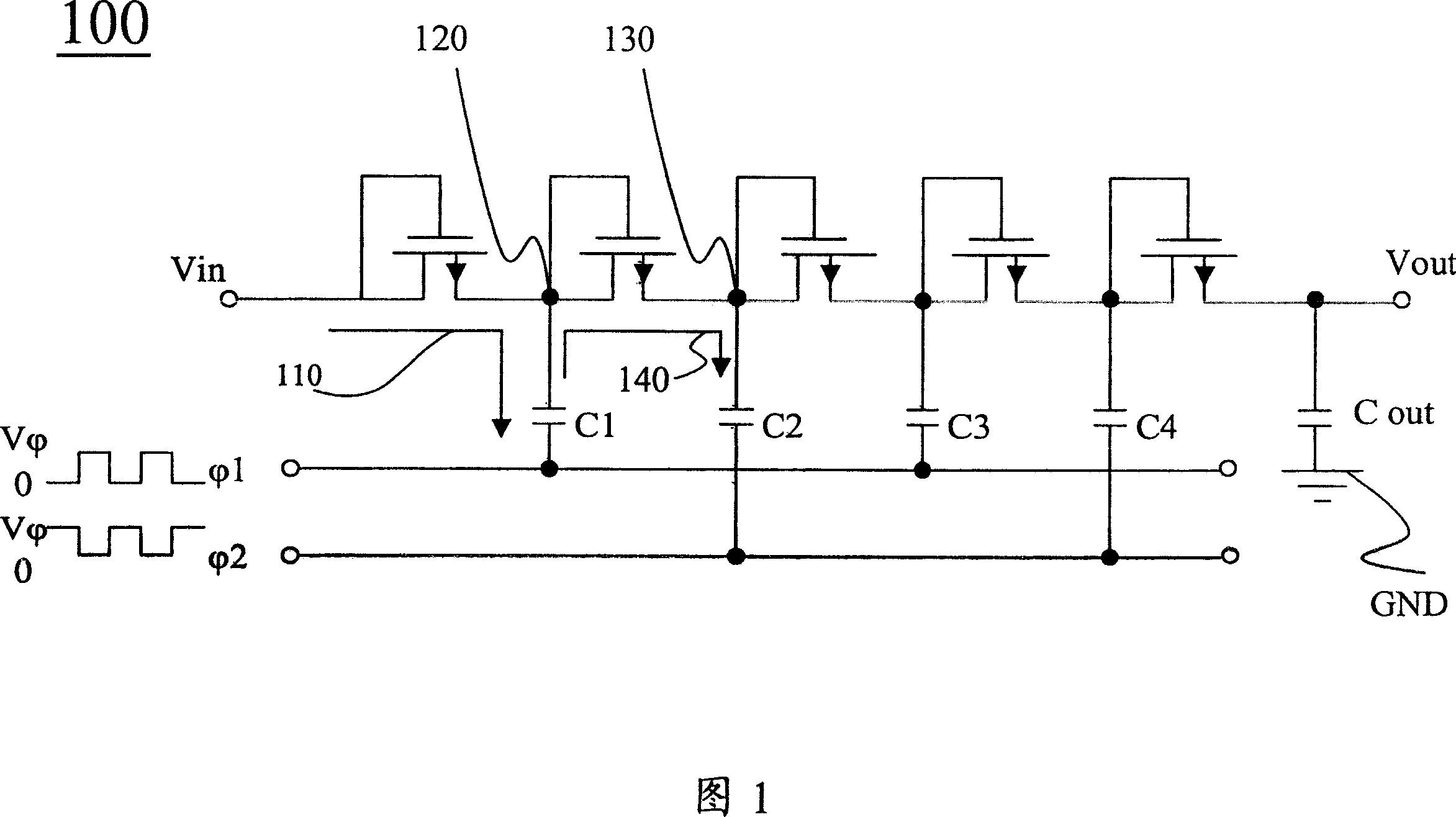
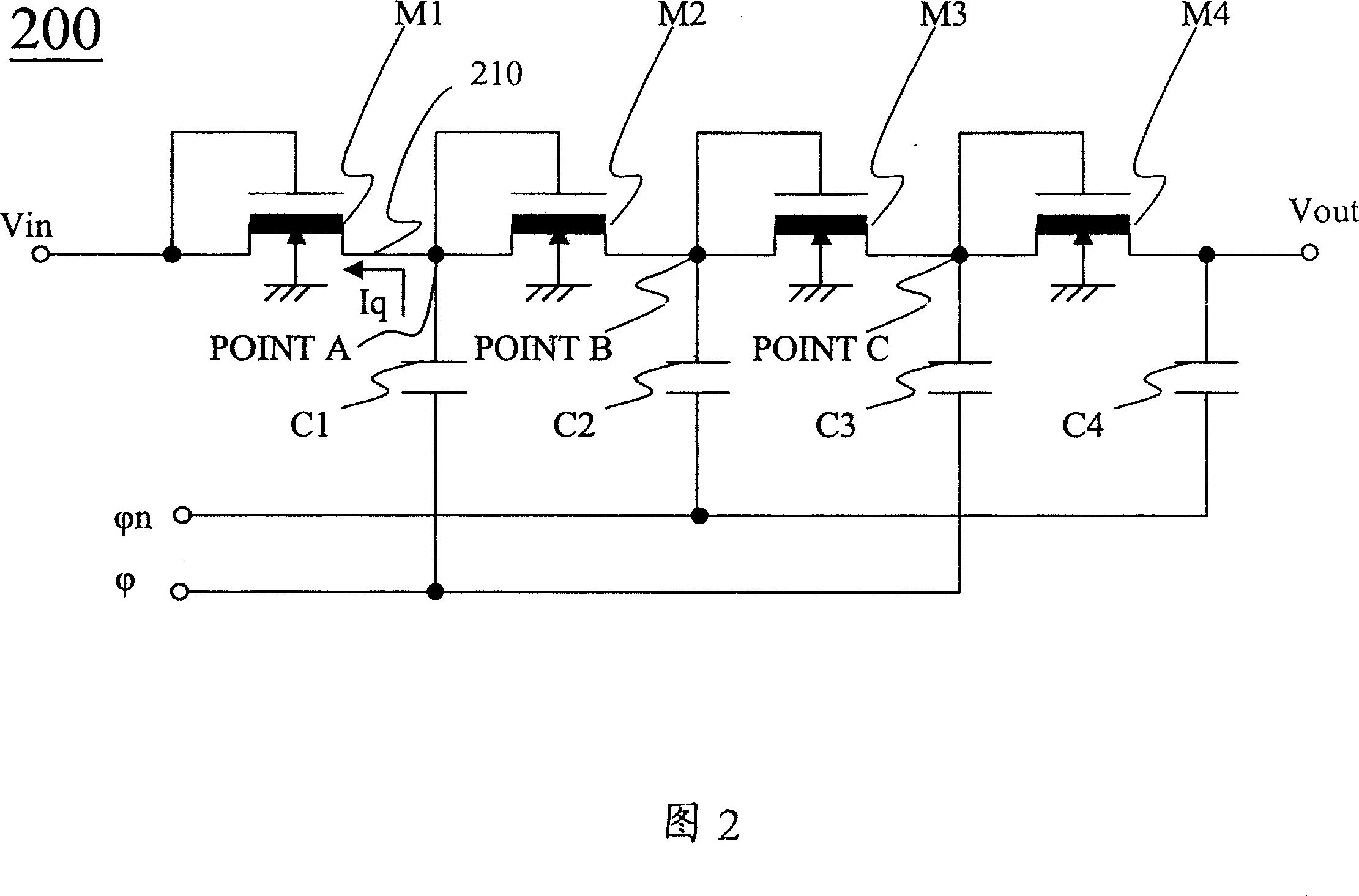
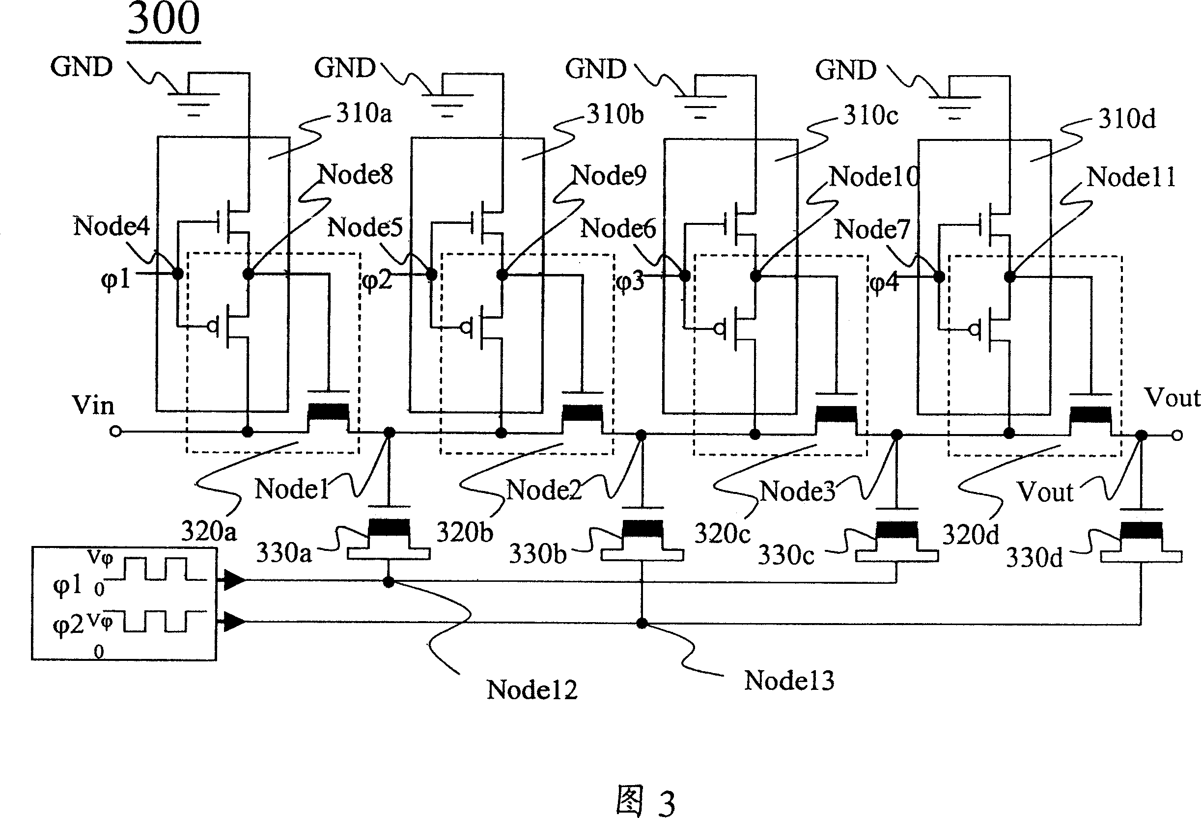
[0039]FIG. 3 is a schematic diagram of a four-order boost charge boosting circuit (4-order Chareg-pump Circuit) 300 disclosed in one of the embodiments of the present invention. The four-order boost charge boost circuit 300 includes a A first reverse current cut-off circuit 310a, a second reverse current cut-off circuit 310b, a third reverse current cut-off circuit 310c, a fourth reverse current cut-off circuit 310d, a first equivalent diode 320a, a second equivalent diode 320b , a third equivalent diode 320c, a fourth equivalent diode 320d, a first boost capacitor 330a, a second boost capacitor 330b, a third boost capacitor 330c and a fourth boost capacitor 330d, wherein Each reverse current cut-off circuit 310 includes a switch pair. In this embodiment, the reverse current cut-off circuit 310 is respectively composed of an enhanced N-channel metal oxide semiconductor transistor (Enhancement-type N-channel Transistor) and an enhanced P channel metal oxide transistor. Semicond...


PUM


Abstract

The utility model relates to an electric charge boosting circuit, comprising a plurality of diode equivalent networks, at least a boosting capacitance network and at least one reverse current cut-off circuit; wherein the diode equivalent networks are electrically connected in series with each other; a node is arranged between every two diode equivalent networks and each node is responding to a boosting stage; the low-voltage side of the diode equivalent network with the lowest boosting stage is the input of the electric charge boosting circuit and the input receives an input voltage signal; one end of each boosting capacitance network is connected with a node and the other end of each boosting capacitance network is electrically connected with a clock signal; each reverse current cut-off circuit is electrically connected with the diode equivalent network; the reverse current cut-off circuit is provided with at least two break-over channels, which are alternately turned on according to the clock signal switch in each boosting stage.

Description

technical field [0001] The invention relates to a charge boosting circuit, in particular to a charge boosting circuit which uses a reverse current cut-off circuit to improve circuit efficiency and reliability. Background technique [0002] The charge booster circuit (Charge Pump) is a circuit that realizes buck-boost through the charge accumulation effect on the capacitor. With the development of various types of portable memory and flash memory applications, it is becoming more and more common that the operating voltage required by the system is higher than the power supply voltage. The resulting power management problems can be solved by using a boost charge booster circuit . A step-up type charge boosting circuit can stabilize the step-down voltage or generate an output higher than the power supply voltage. Please refer to FIG. 1, which is a schematic diagram of an existing dual phase charge boosting circuit 100. The charge boosting circuit 100 It includes a group of n-...

Claims


Application Information

Patent Timeline
IPC IPC(8): H02M3/07
Inventor 吴哲铭吴盈锋
Owner G TIME ELECTRONICS
Why Eureka
Try Eureka