Boost circuit and switching power supply

A booster circuit and circuit technology, applied in electrical components, regulating electrical variables, instruments, etc., can solve the problems of short-term simultaneous conduction of the first switch group and second switch group, short-circuit of the booster circuit, damage to the booster circuit, etc.

Pending Publication Date: 2022-04-12
SHANGHAI AWINIC TECH CO LTD
View PDF0 Cites 0 Cited by
  • Summary
  • Abstract
  • Description
  • Claims
  • Application Information

AI Technical Summary

Problems solved by technology

As a result, when the states of the first switch group and the second switch group are switched, the first switch group and the second switch group may be turned on at the same time for a short time, thus causing the output terminal of the boost circuit to be short-circuited, resulting in A large series current reduces the boosting efficiency of the boosting circuit, and may even damage the boosting circuit

Method used


Image

  • Boost circuit and switching power supply
  • Boost circuit and switching power supply
  • Boost circuit and switching power supply

Examples


Embodiment Construction

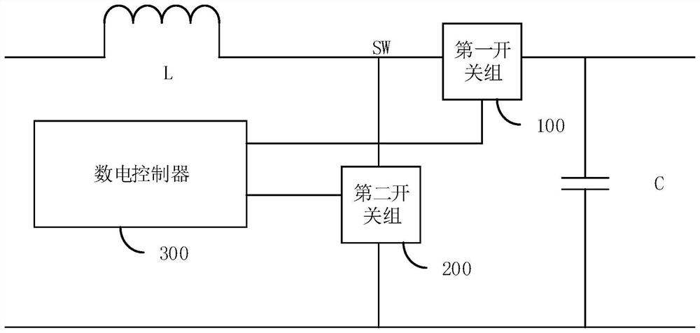
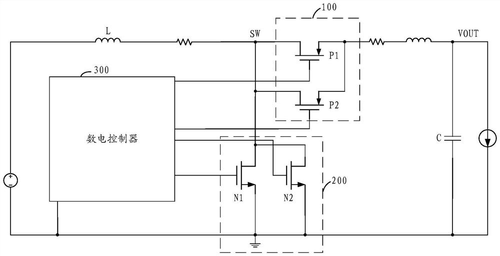
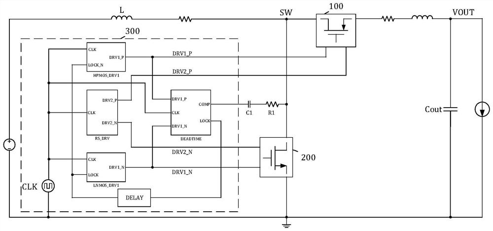
[0047] With the rapid development of microelectronics technology, the requirements for the boost circuit are getting higher and higher. The voltage boosting circuit realizes voltage boosting mainly by controlling the first switch group and the second switch group therein. When the first switch group is turned off, the second switch group is turned on, and the inductance in the boost circuit stores energy; when the first switch group is turned on, the second switch group is turned off, and the inductance in the boost circuit to charge.

[0048] In order to improve the efficiency of the boost circuit, the on-resistance of the switching elements in the current boost circuit is very small. As a result, when the states of the first switch group and the second switch group are switched, the first switch group and the second switch group may be turned on at the same time for a short time, thus causing the output terminal of the boost circuit to be short-circuited, resulting in A la...


PUM


Abstract

The invention discloses a booster circuit, which comprises an inductor, an output capacitor, a first switch group, a second switch group and a digital power controller, the switch tubes in the first switch group are connected in parallel, and the switch tubes in the second switch group are connected in parallel; the inductor is connected with the first end of the first switch group and the first end of the second switch group. The second end of the first switch group is connected with the first end of the output capacitor; the second end of the output capacitor is grounded; the second end of the second switch group is grounded; and the digital electric controller is used for controlling the switch tubes in the second switch group to be switched on after all the switch tubes in the first switch group are switched off for a first preset time, or controlling the switch tubes in the first switch group to be switched on after all the switch tubes in the second switch group are switched off for the first preset time. The situation that switch tubes of the first switch group and the second switch group are switched on at the same time is avoided, the boost efficiency of the boost circuit is improved, and meanwhile the boost circuit is prevented from being damaged by series current.

Description

technical field [0001] The present application relates to the field of power supplies, in particular to a boost circuit and a switching power supply. Background technique [0002] With the rapid development of microelectronics technology, the requirements for the boost circuit are getting higher and higher. The voltage boosting circuit realizes voltage boosting mainly by controlling the first switch group and the second switch group therein. When the first switch group is turned off, the second switch group is turned on, and the inductance in the boost circuit stores energy; when the first switch group is turned on, the second switch group is turned off, and the inductance in the boost circuit to charge. [0003] In order to improve the efficiency of the boost circuit, the on-resistance of the switching elements in the current boost circuit is very small. As a result, when the states of the first switch group and the second switch group are switched, the first switch grou...

Claims


Application Information

Patent Timeline
Patent Type & Authority Applications(China)
IPC IPC(8): H02M3/158H02M1/08
Inventor 王益峰袁政
Owner SHANGHAI AWINIC TECH CO LTD
Why Eureka
Try Eureka