Display device

a display device and display technology, applied in semiconductor devices, instruments, optics, etc., can solve the problems of reducing affecting the appearance of the pixel, and often rendering parts or all of the code impossible or difficult to view, so as to reduce the area of the frame region, and reduce the area of the componen

Active Publication Date: 2010-10-12
SHARP KK
View PDF16 Cites 3 Cited by
  • Summary
  • Abstract
  • Description
  • Claims
  • Application Information

AI Technical Summary

Benefits of technology

[0041]According to the first aspect of the invention, the area of the component included in the dummy pixel portions is smaller than that of each of the components included in the pixel formation portions, and therefore, for example, it is possible to note a code of a required size in the dummy pixel portions. Thus, it is possible to provide a display device with a reduced frame region required for the dummy pixel portions and code notation.
[0042]According to the second aspect of the invention, the repair portion, the memory circuit, or the sensor circuit, which is included in the pixel formation portions as their component, is not included in the dummy pixel portions, and therefore it is possible to reduce the area of the component included in the dummy pixel portions.
[0043]According to the third aspect of the invention, the semiconductor layer in the dummy pixel portions is smaller in area than that in the pixel formation portions, and therefore it is possible to further reduce the area of the component included in the dummy pixel portions, making it possible to conveniently change the position of the contact hole coupled to the semiconductor layer, for example.
[0044]According to the fourth aspect of the invention, the second thin film transistor included in the dummy pixel portions has a lesser number of gate electrodes than the number of gate electrodes in the first thin film transistor included in the pixel formation portions, and therefore it is possible to further reduce the area of the component included in the dummy pixel portions.
[0045]According to the fifth aspect of the invention, the dummy pixel portions each include only an electrode connected to one of the two electrodes included in the storage capacitance portion of the pixel formation portion adjacent thereto, so that there is no region where light is blocked by the other electrode, making it possible to further reduce the area of the light blocking effect component included in the dummy pixel portion.
[0046]According to the sixth aspect of the invention, the dummy pixel portions each include an electrode (e.g., a storage capacitance line electrode) having a smaller width than that of one of the electrodes included in the pixel formation portions, and therefore a region where light is blocked by that electrode is reduced in size, making it possible to further reduce the area of the light blocking effect component included in the dummy pixel portion.

Problems solved by technology

For example, if a predetermined potential from the source bus line 160 cannot be written onto the pixel electrode for such a reason that the thin film transistor in the pixel formation portion has been disconnected during manufacture, such a defective pixel formation portion is undesirable because it appears as a bright spot (in the case of a normally-white-type display device).
Also, in such a case, part or all of the code is often rendered impossible or hard to view even from the counter board 200 side.

Method used


Image

  • Display device
  • Display device
  • Display device

Examples


Embodiment Construction

[0098]Hereinafter, an embodiment of the present invention and variants thereof will be described with reference to the accompanying drawings.

[0099]

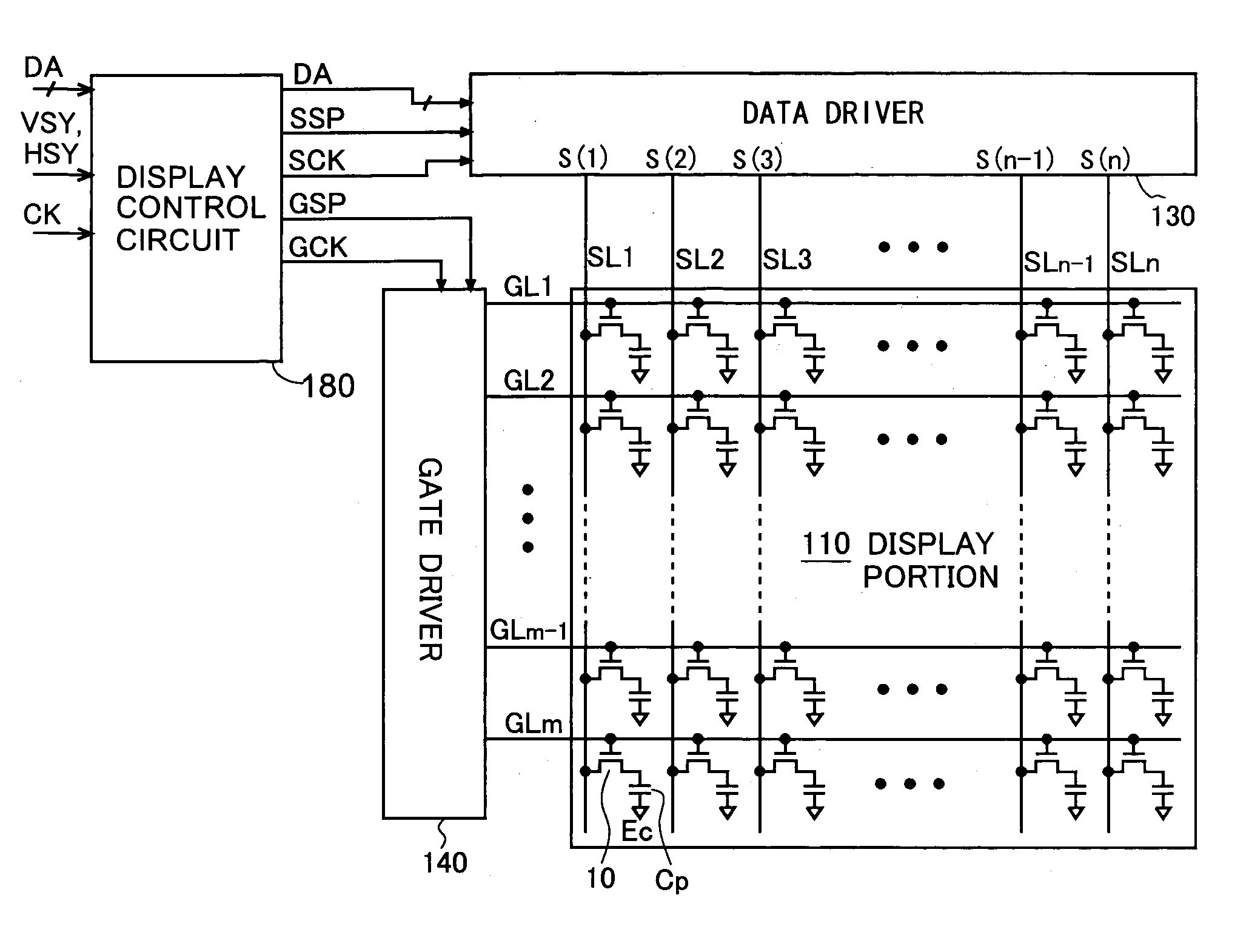
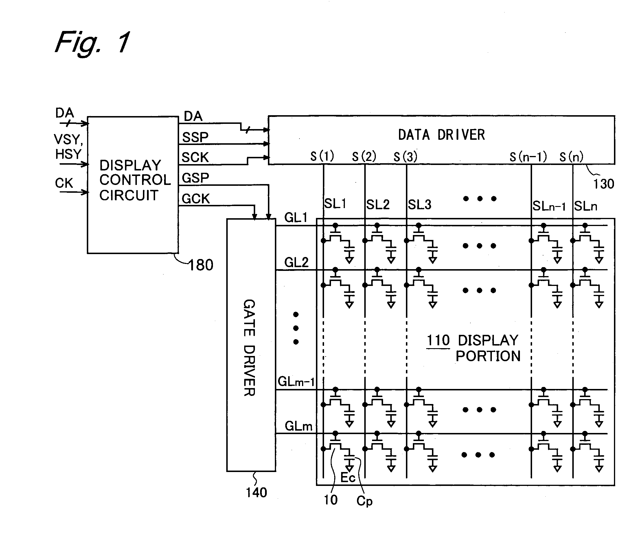
[0100]First, the configuration and operation of a liquid crystal display device according to an embodiment of the present invention will be described with reference to FIG. 1.

[0101]FIG. 1 is a block diagram illustrating the configuration of the liquid crystal display device according to the present embodiment, along with an equivalent circuit of a display portion thereof. As shown in FIG. 1, the liquid crystal display device includes an active matrix display portion (display region) 110, a source driver 130 acting as a video signal line drive circuit, a gate driver 140 acting as a scanning signal line drive circuit, and a display control circuit 180 for controlling the source driver 130 and the gate driver 140. Since the overall structure of the display device is similar to the above-described structure shown in FIG. 11, the same elements...


PUM

PropertyMeasurementUnit
sizeaaaaaaaaaa
areaaaaaaaaaaa
storage capacitanceaaaaaaaaaa

Abstract

The present invention realizes a display device with dummy pixel portions and a frame region required for the dummy pixel portions and code notation, in which the frame region is minimized while achieving code notation in required size.In a dummy pixel portion (122) of the present display device, the number of gate electrodes in a thin film transistor formed by a semiconductor layer (11) is reduced to two, so that distances from a contact hole (12) to another contact hole (13) and to a through-hole (14) can be shortened as compared to those in pixel formation portions (112a, 112b), making it possible to dispose the contact hole (13) and the through-hole (14) in a lower portion in the figure. In addition, provided in the vicinity of the center of the dummy pixel portion (122) is only an electrode equivalent to a storage capacitance line (170). Thus, a wide transparent region can be ensured to note a code (22) of a sufficient size in the dummy pixel portion (122).

Description

TECHNICAL FIELD[0001]The present invention relates to display devices, and more specifically to a display device in which liquid crystal elements or EL (electro luminescence) elements are disposed in the form of a matrix.BACKGROUND ART[0002]In recent years, flat-panel display devices as typified by liquid crystal display devices have been in practical use, and mounted in a variety of types of electronic equipment, in particular mobile electronic equipment. Widely-used flat-panel liquid crystal display devices are thin liquid crystal display devices of active matrix type capable of high-resolution display.[0003]FIG. 11 is a view schematically illustrating the structure of such a conventional active matrix liquid crystal display device. The active matrix liquid crystal display device is composed of two boards having a liquid crystal layer sandwiched there between, in which an element board 100, one of the two boards, has disposed thereon in the form of a lattice a plurality of unillus...

Claims


Application Information

Patent Timeline
Patent Type & Authority Patents(United States)
IPC IPC(8): G02F1/1345
CPCG02F1/136227G02F1/136259G02F1/133555G02F1/13454G02F2001/133374G02F2001/133388G02F2001/136268G02F1/133374G02F1/133388G02F1/136268
Inventor FUJIKAWA, YOHSUKE
Owner SHARP KK
Why Eureka
Try Eureka