Liquid crystal display device

a liquid crystal display and display device technology, applied in non-linear optics, instruments, optics, etc., can solve the problems of difficult control of the end of the applied material, difficult control of the application, and poor bonding reliability so as to ensure the bonding strength of the seal material, reduce the frame region, and excellent image quality

Active Publication Date: 2016-06-07
JAPAN DISPLAY INC
View PDF8 Cites 1 Cited by
  • Summary
  • Abstract
  • Description
  • Claims
  • Application Information

AI Technical Summary

Benefits of technology

[0016]The invention provides a liquid crystal display device including the photo-alignment processed alignment film, which reduces the frame region, secures reliability of the seal portion, and provides no uneven brightness of the region around the display screen.
[0019]The invention ensures bonding strength of the seal material to the TFT substrate or the counter substrate, and even film thickness of the alignment film on the display region. This makes it possible to realize the liquid crystal display device with a reduced frame region and excellent image quality as well as reliability at the seal portion.

Problems solved by technology

Meanwhile, presence of the alignment film between the seal material and the TFT substrate or between the seal material and the counter substrate may impair bonding reliability of the seal material.
On the contrary, the liquid crystal display device of IPS type that requires no pre-tilt angle is suitable for the photo-alignment process.
It is therefore difficult to control the end of the applied material.
Especially when applying the alignment film through ink jetting, it is further difficult to control the application because of low viscosity of the material for forming the alignment film.
This may cause uneven brightness especially around the display screen.

Method used


Image

  • Liquid crystal display device
  • Liquid crystal display device
  • Liquid crystal display device

Examples


first embodiment

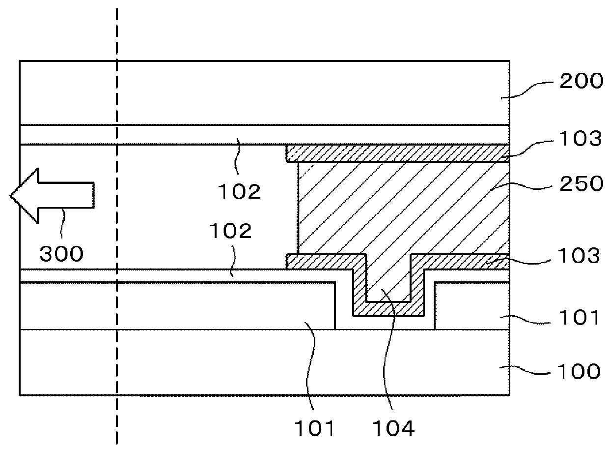
[0036]FIG. 1 is a sectional view illustrating a first embodiment of the invention. An organic passivation film 101 with a recess or an eliminated portion 104 is formed on a TFT substrate 100, and an alignment film 102 is further formed on the organic passivation film. The aforementioned structure is similar to the one described referring to FIG. 13 as well as the function of the recess 104. The gate insulation film, the inter-layer insulation film and the like formed on the TFT substrate 100 are omitted in the drawing as already explained referring to FIG. 13. The structure applies to the following embodiments unless otherwise specified.

[0037]Referring to FIG. 1, the structure having the alignment film 102 formed on the counter substrate 200 is also similar to the one described referring to FIG. 13. Films including the color filter, black matrix, overcoat film and the like formed on the counter substrate 200 are omitted in the drawing as already explained referring to FIG. 13. The r...

second embodiment

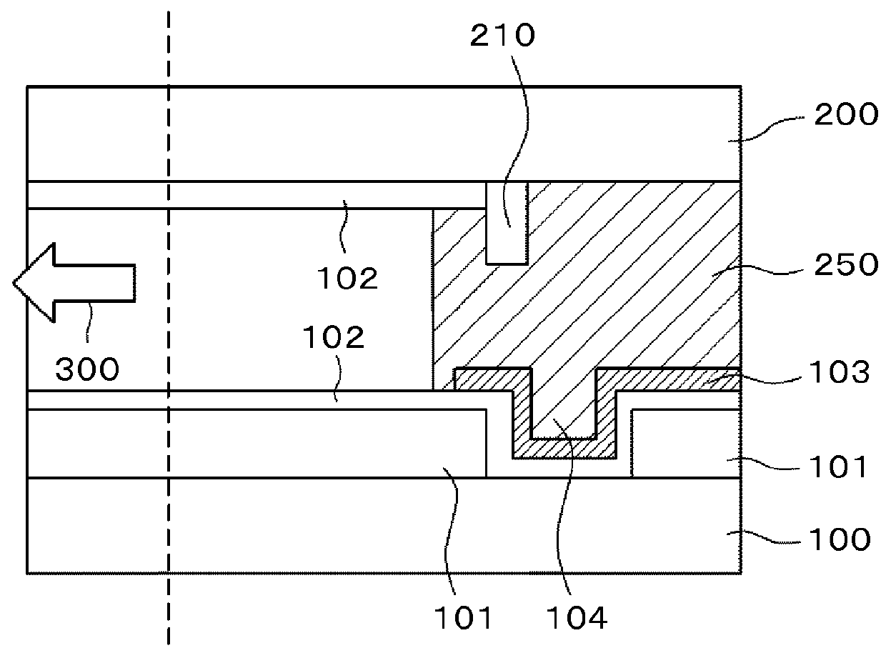
[0057]FIG. 3 is a sectional view of a part around a seal portion of a liquid crystal display panel according to a second embodiment of the invention. Referring to FIG. 3, the part at the side of the TFT substrate 100 is similar to that of the second example of the first embodiment as shown in FIG. 2. The structure shown in FIG. 3 is different from the one shown in FIG. 2 in the part at the side of the counter substrate 200. At the side of the counter substrate 200, the range for applying the alignment film 102 is controlled by an alignment film barrier 210 formed through the same process for forming a columnar spacer. The columnar spacer is formed on the counter substrate 200 to regulate the distance between the TFT substrate 100 and the counter substrate 200. For example, acrylic resin is available as the material for forming the columnar spacer. It is possible to form the alignment film barrier 210 with its height smaller than that of the columnar spacer formed on the display regi...

third embodiment

[0065]FIG. 6 is a sectional view of the liquid crystal display panel according to a third embodiment of the invention at a part around the seal portion. Referring to FIG. 6, the display region 300 at the TFT substrate 100 and the counter substrate 200 is defined by the alignment film 102. The part in contact with the seal material 250 is formed by a mixture film 105 as a mixture of the alignment film 102 and the organic film 103. As FIG. 6 shows, the part indicated by the white arrow is the display region 300. The mixture film 105 has only a small component to be photo-aligned. Therefore, the degree of deterioration of the film caused by the ultraviolet light for the photo-alignment process is low, thus ensuring bonding strength to the seal material 250.

[0066]FIG. 7 is a plan view of the part at the side of the TFT substrate 100 according to the embodiment. Referring to FIG. 7, the alignment film 102 is formed on the display region, and the mixture film 105 is formed outside. The se...


PUM

PropertyMeasurementUnit
wavelengthaaaaaaaaaa

Abstract

A TFT substrate and a counter substrate are bonded via a seal material. Alignment films are applied to entire surfaces of the TFT substrate and the counter substrate so as to realize even thickness of the alignment film. This allows a display region to be formed up to the area around the seal material. The alignment film is photo-alignment processed. An organic film formed of the material which is not photo-aligned is interposed between the alignment film and the seal material. High bonding strength between the organic film and the seal material improves reliability of a seal portion as well as reduces a frame region.

Description

BACKGROUND OF THE INVENTION[0001](1) Field of the Invention[0002]The invention relates to a display device. More specifically, the invention relates to a liquid crystal display device capable of increasing a display region relative to a predetermined outline region, that is, realizing a narrow frame through the photo-alignment process.[0003](2) Description of the Related Art[0004]The liquid crystal display device is configured to include a TFT substrate in which pixels with pixel electrodes and thin film transistors (TFT) arranged in a matrix, and a counter substrate opposite the TFT substrate, having a color filter and the like formed at a location corresponding to the pixel electrode of the TFT substrate. A liquid crystal is interposed between the TFT substrate and the counter substrate. An image is formed by controlling light transmittance of the liquid crystal molecule for each pixel.[0005]The liquid crystal display device with a flat and light structure has been widely used in ...

Claims


Application Information

Patent Timeline
Patent Type & Authority Patents(United States)
IPC IPC(8): G02F1/1337G02F1/1339G02F1/1333
CPCG02F1/133788G02F1/1339G02F1/133345G02F1/1337
Inventor KUNIMATSU, NOBORUTOMIOKA, YASUSHISONODA, HIDEHIROHYODO, YOSUKEIMANISHI, YASUO
Owner JAPAN DISPLAY INC
Why Eureka
Try Eureka