Image display device with frame region transistor control line including stacked line layers

a display device and transistor control technology, applied in the field of image display devices, can solve the problems of display defects, uneven brightness in the form of blocks for each segment, etc., and achieve the effect of reducing the frame region

Active Publication Date: 2020-11-17
SHARP KK
View PDF10 Cites 0 Cited by
  • Summary
  • Abstract
  • Description
  • Claims
  • Application Information

AI Technical Summary

Benefits of technology

[0026]The present invention can provide an image display device with a reduced frame region.

Problems solved by technology

In this structure, display defects (e.g., uneven brightness in the form of blocks for each segment) tend to occur particularly at a position far from the driver mounting portion.

Method used


Image

  • Image display device with frame region transistor control line including stacked line layers
  • Image display device with frame region transistor control line including stacked line layers
  • Image display device with frame region transistor control line including stacked line layers

Examples


embodiment 1

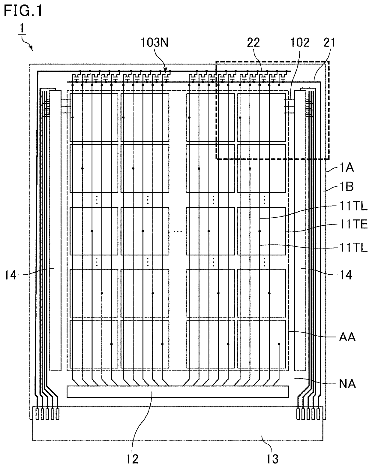
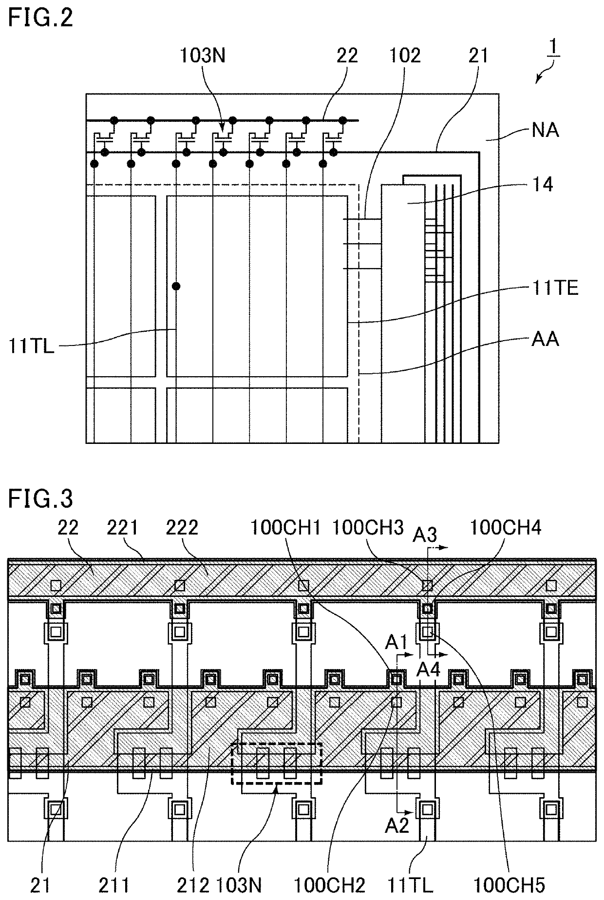
[0093]FIG. 1 is a schematic plan view of a liquid crystal display device of Embodiment 1. FIG. 2 is an enlarged schematic plan view of the region surrounded by the dashed line in FIG. 1. As shown in FIG. 1 and FIG. 2, a liquid crystal display device 1 of the present embodiment includes a display region AA for displaying an image and a frame region NA which is a peripheral region of the display region AA. The liquid crystal display device 1 also includes a thin-film transistor substrate (hereinafter, also referred to as TFT substrate) 1A, a counter substrate 1B facing the TFT substrate 1A, and a liquid crystal layer (not shown) between the TFT substrate 1A and the counter substrate 1B. The TFT substrate 1A in the present embodiment is also referred to as an array substrate.

[0094]The liquid crystal display device 1 includes a first alignment film (not shown) between the TFT substrate 1A and the liquid crystal layer; a second alignment film (not shown) between the counter substrate 1B ...

embodiment 2

[0142]In the present embodiment, features unique to the present embodiment are mainly described, and the same features as those in the above embodiment are not described again. The liquid crystal display device of the present embodiment is assumed to be a FFS mode liquid crystal display device as in the above embodiment. Described in Embodiment 1 is a structure where one common signal line is disposed and the conductive lines are TP lines. Described in the present embodiment is a structure where multiple common signal lines are disposed and the conductive lines are inspection lines.

[0143]FIG. 9 is a schematic plan view of a liquid crystal display device of Embodiment 2, with a first line layer and a second line layer highlighted. FIG. 10 is a schematic plan view of the liquid crystal display device of Embodiment 2, with a third line layer highlighted. FIG. 11A to FIG. 11D are schematic cross-sectional views of a TFT substrate in the liquid crystal display device of Embodiment 2. FIG...

embodiment 3

[0159]In the present embodiment, features unique to the present embodiment are mainly described, and the same features as those in the above embodiments are not described again. The liquid crystal display device of the present embodiment is assumed to be a FFS mode liquid crystal display device as in Embodiment 1. Described in Embodiment 1 is a structure including the driver 12 for both data signals and touch sensors and the FPC 13 disposed in one side area of the frame region NA and the gate drive circuit 14 is monolithically formed in each of two side areas of the frame region NA. In the present embodiment, the driver 12 for both data signals and touch sensors and the FPC 13 are disposed in one side area of the frame region NA, and a gate driver is mounted in another side area of the frame region NA.

[0160]FIG. 12 is a schematic plan view of a liquid crystal display device of Embodiment 3. As shown in FIG. 12, the liquid crystal display device 1 of the present embodiment includes t...


PUM

PropertyMeasurementUnit
sizeaaaaaaaaaa
sizeaaaaaaaaaa
sizeaaaaaaaaaa

Abstract

The present invention provides an image display device which includes a substrate; a display region; and a frame region. The substrate includes a first line layer, a second line layer, and a third line layer; thin-film transistors disposed in the frame region; a control line disposed in the frame region and connected to a gate electrode of each of the thin-film transistors; a common signal line disposed in the frame region and connected to one of a source electrode or a drain electrode of each of the thin-film transistors; and conductive lines each connected to the other of each of the thin-film transistors and extending from the frame region into the display region. The control line includes a first control line portion in the first line layer, a second control line portion in the second line layer, and a third control line portion in the third line layer.

Description

CROSS-REFERENCE TO RELATED APPLICATIONS[0001]The present application claims priority under 35 U.S.C. § 119 to U.S. Provisional Patent Application No. 62 / 730,021 filed on Sep. 12, 2018, the contents of which are incorporated herein by reference in their entirety.BACKGROUND OF THE INVENTIONField of the Invention[0002]The present invention relates to image display devices. More specifically, the present invention relates to an image display device including thin-film transistors in a frame region.Description of Related Art[0003]Image display devices such as liquid crystal display devices typically include a thin-film transistor substrate (hereinafter, also abbreviated to TFT substrate) including many thin-film transistors (hereinafter, also abbreviated to TFTs). Some recent image display devices including a TFT substrate are equipped with an in-cell touch panel which is a display panel having a touch panel function.[0004]Regarding an image display device including an in-cell touch pane...

Claims


Application Information

Patent Timeline
Patent Type & Authority Patents(United States)
IPC IPC(8): G02F1/1362G02F1/133G02F1/1333G06F3/041
CPCG06F3/0412G06F3/0416G02F1/133308G02F1/13338G02F1/13306G02F1/136286G02F2001/13629G02F1/13454G06F2203/04103G06F3/04164G06F3/04166G06F3/0443G02F1/13629
Inventor YOSHIDA, MASAHIRO
Owner SHARP KK
Why Eureka
Try Eureka