Image display device

a display device and image technology, applied in semiconductor devices, instruments, optics, etc., can solve the problems of limitation of frame design, difficult reduction of frame region, etc., and achieve the effect of suppressing the reduction of the aperture ratio of the display region and reducing the frame region

Active Publication Date: 2020-06-30
SHARP KK
View PDF9 Cites 0 Cited by
  • Summary
  • Abstract
  • Description
  • Claims
  • Application Information

AI Technical Summary

Benefits of technology

[0013]JP 2016-186649 A discloses that, in the liquid crystal display device disclosed in FIG. 3 and FIG. 5B, for example, at least a part of the gate driver (a thin-film transistor or the like as a switching element) is arranged in a pixel region (corresponding to a display region), and thereby the frame can be narrowed compared to the case where all the gate drivers are arranged outside the pixel region. However, the gate driver provided in the liquid crystal display device of JP 2016-186649 A is arranged between the gate line and the gate line in the display region, and an aperture ratio of the display region may be reduced.
[0014]The present invention has been made in view of such a current state of the art and aims to provide an image display device capable of reducing a frame region and suppressing a reduction in the aperture ratio of the display region while providing at least a part of a gate driver monolithically in the frame region.
[0028]The present invention can provide an image display device capable of reducing a frame region and suppressing a reduction in the aperture ratio of the display region while providing at least a part of a gate driver monolithically in the frame region.

Problems solved by technology

In an image display device provided with the GDM circuit, reducing a region (frame region) in which the GDM circuit is arranged is difficult, particularly in the case of a high definition model.
In the case of a GDM circuit including a TFT using amorphous silicon (hereinafter referred to as a-Si) or an InGaZnO oxide semiconductor, in the same manner as in an output control transistor region DR in which the output control TFT is formed, the size of a bootstrap capacitor region CapAR in which a bootstrap capacitor is formed is large, which is a limitation of the frame design.

Method used


Image

  • Image display device
  • Image display device
  • Image display device

Examples


embodiment 1

[0047]In the present embodiment, an image display device will be described by taking a liquid crystal display device as an example. More specifically, a liquid crystal display device of an FFS (Fringe Field Switching) mode, which is a kind of horizontal alignment mode in which liquid crystal molecules are aligned in a substantially horizontal direction with respect to the main surface of the substrate in the voltage non-applied state, will be described as an example.

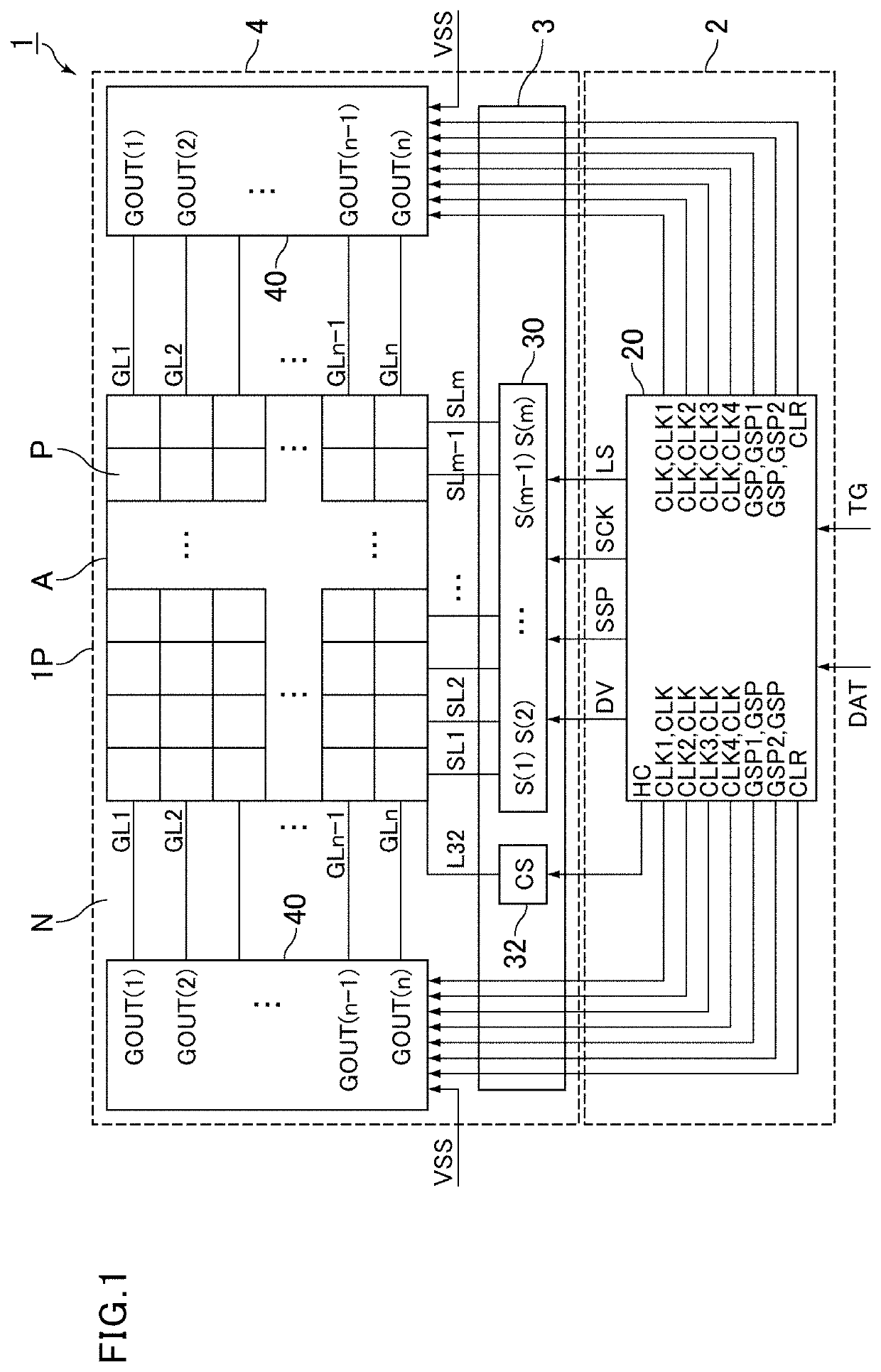
[0048]FIG. 1 is a block diagram showing the entire configuration of the liquid crystal display device of Embodiment 1. As shown in FIG. 1, a liquid crystal display device 1 of Embodiment 1 includes a liquid crystal display panel 1P as a display panel, and a control substrate 2. The liquid crystal display panel 1P has a display region A in which an image is displayed and a frame region N which is a region outside the display region A. The control substrate 2 is provided with a display control circuit 20.

[0049]The liquid c...

embodiment 2

[0120]In the present embodiment, characteristics peculiar to the present embodiment will mainly be described, and description of contents overlapping with the above embodiment will be omitted. The second additional line L20 in Embodiment 1 is electrically connected to the scanning signal line GL, but a second additional line L20 in the present embodiment is not electrically connected to a scanning signal line GL.

[0121]FIG. 14 is a schematic plan view for describing a contact between a scanning signal line and a second additional line provided in a liquid crystal display device of Embodiment 2. As shown in FIG. 14, the second additional line L20 is not electrically connected to the scanning signal line GL overlapping with the second additional line L20. When the pixel size is small, providing a contact hole may be difficult in securing the aperture ratio. In such a case, the reduction of an aperture ratio can be further suppressed by keeping the second additional line L20 and the sca...

modification 1

[0124]In the above embodiments, the gate drivers 40 are respectively arranged in the left and right frame regions N via the display region A, and the liquid crystal display device 1 includes the two gate drivers 40. However, the gate driver 40 may be arranged only in the frame region N on one side of the display region A, and the number of gate drivers 40 provided in the liquid crystal display device 1 may be one. For example, when one gate driver 40 is arranged in the left frame region N, each scanning signal line GL overlaps a first additional line L10 in the left frame region N and the left side part of the display region A, and overlaps a second additional line L20 in the right side part of the display region A via a gap portion GAP1. Thus, in the case where one gate driver 40 is provided, substantially the entire region in the lengthwise direction (longitudinal direction) of each scanning signal line GL except for at least one gap portion GAP1 preferably overlaps the first addi...


PUM

PropertyMeasurementUnit
sizeaaaaaaaaaa
conductiveaaaaaaaaaa
voltageaaaaaaaaaa

Abstract

The image display device of the present invention includes a substrate. The substrate includes: a first metal layer, a first insulating layer, a second metal layer, a second insulating layer, and a third metal layer stacked in the stated order; a scanning signal line; and a gate driver. The gate driver includes a unit circuit including an output control transistor. The scanning signal line is provided in the second metal layer in the display region. The substrate includes a first additional line electrically connected to a gate electrode of the output control transistor. The first additional line includes a first additional line portion provided in the first metal layer in the display region. The first additional line portion overlaps the scanning signal line in the display region via the first insulating layer.

Description

CROSS-REFERENCE TO RELATED APPLICATIONS[0001]The present application claims priority under 35 U.S.C. § 119 to U.S. Patent Application No. 62 / 691,665 filed on Jun. 29, 2018, the contents of which are incorporated herein by reference in their entirety.BACKGROUND OF THE INVENTIONField of the Invention[0002]The present invention relates to an image display device. More particularly, the present invention relates to an image display device including a gate driver monolithically provided on an insulating substrate.Description of Related Art[0003]As one of the image display devices, an active matrix liquid crystal display device which includes a display region including multiple video signal lines (data lines) and multiple scanning signal lines (gate lines) is known. Generally, an active matrix liquid crystal display device displays an image by selecting pixels arranged in a matrix in units of row and writing a voltage corresponding to display data to the selected pixels. Conventionally, i...

Claims


Application Information

Patent Timeline
Patent Type & Authority Patents(United States)
IPC IPC(8): G09G3/36G02F1/1362G02F1/133G02F1/1368G02F1/1345G09G3/30G02F1/1333
CPCG02F1/13454G02F1/13306G02F1/136286G02F1/1368G02F1/133308G02F1/133345G09G3/3677G09G2300/08G09G2300/0426G09G2300/0408H01L27/1244H01L27/1255G09G2310/0267G09G2310/0286
Inventor YOSHIDA, MASAHIRO
Owner SHARP KK
Why Eureka
Try Eureka