Test interface for memory elements

a memory element and interface technology, applied in the field of integrated circuit testing, can solve the problems of excessive test time, insufficient mux stage, and specifically the corresponding propagation delay,

Inactive Publication Date: 2010-11-30
INT BUSINESS MASCH CORP
View PDF8 Cites 6 Cited by
  • Summary
  • Abstract
  • Description
  • Claims
  • Application Information

AI Technical Summary

Benefits of technology

[0006]The present invention solves the foregoing problems by providing an array built in self test (ABIST) interface for testing memory elements of an integrated circuit and a method of creating and using the same. In particular, the ABIST interface of the invention may provide a multiplexer stage at the scan input of each individual functional latch for address, data, and control signals of the memory element under test. In this way, there is no MUX stage positioned in a functional path, and the ABIST signals may be applied in a parallel fashion without impacting the performance of the memory element when in the functional mode of operation.

Problems solved by technology

However, a drawback of this arrangement is that the MUX stage, and specifically the corresponding propagation delay, is in the functional path.
A further drawback is that a MUX stage is required for each individual address, data, and control bit, which results in the consumption of chip real estate and additional power.
However, a major drawback of this arrangement is that the test data from the ABIST engine needs to be scanned into the latches, which may take many cycles (e.g. a number of cycles equal to the number of latches) and, therefore, may result in excessive test times. Furthermore, for specific cycle-to-cycle tests, such as those where two different addresses are read into two consecutive clock cycles, two or more sets of data must be loaded.
As a result, duplication of these latches is required, thus affecting area and power.

Method used


Image

  • Test interface for memory elements
  • Test interface for memory elements
  • Test interface for memory elements

Examples


Embodiment Construction

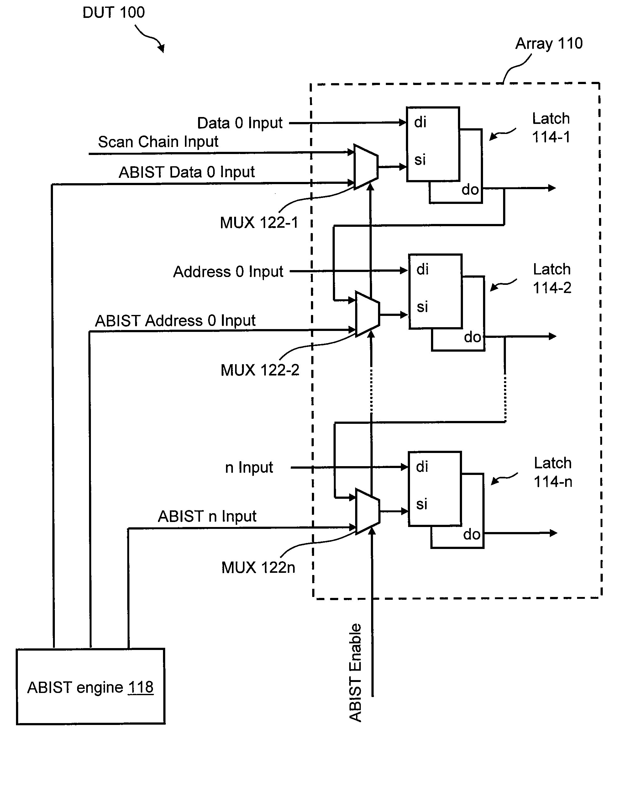
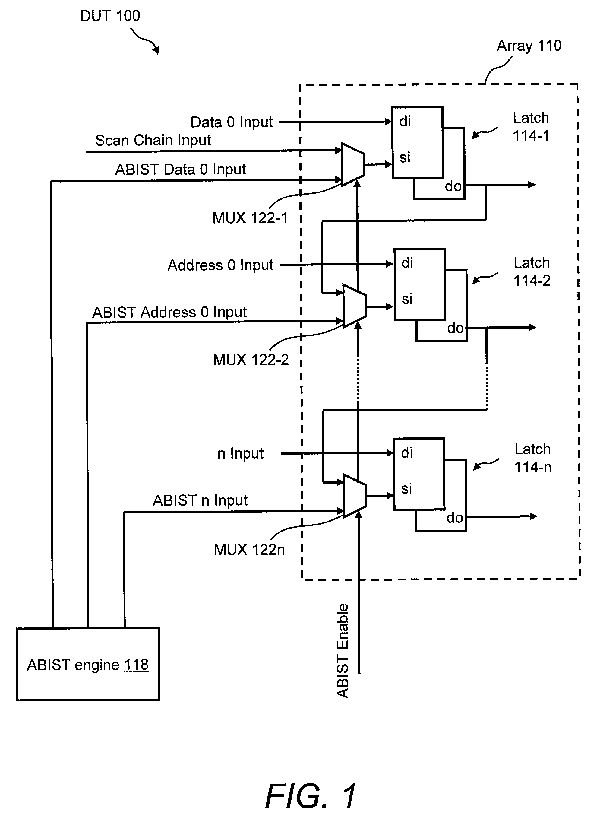
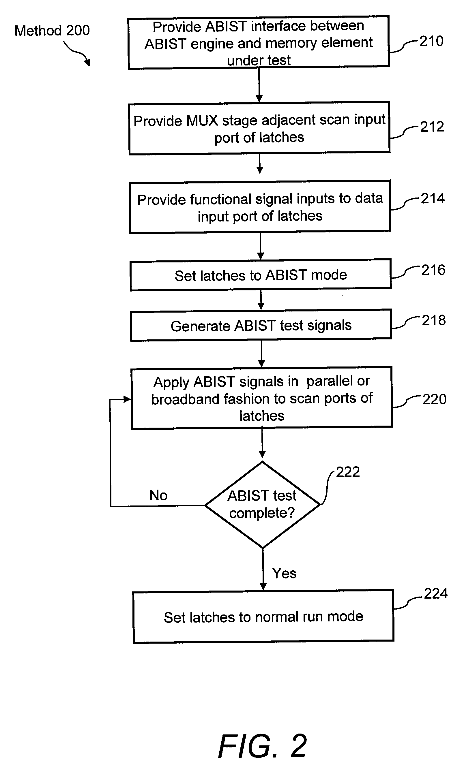
[0012]Generally speaking, the present invention includes an ABIST interface for testing memory elements of an integrated circuit and a corresponding method of creating and using the same. The ABIST interface of the invention may provide a mechanism to interface the ABIST engine to memory elements under test in a manner that does not impact chip performance, minimizes the amount of chip real estate that is needed, minimizes the amount of power consumption, and minimizes test time. In particular, the ABIST interface of the invention may provide a MUX stage at the scan input (i.e., scan port of the latch) of each individual cell of the memory element under test. In this way, the ABIST signals may be applied in a parallel fashion without impacting the performance of the memory element when in the functional mode of operation. Additionally, the ABIST interface of the invention may allow a full set of test patterns to be applied every clock cycle, which may provide maximum flexibility for...


PUM


Abstract

A method for testing memory elements of an integrated circuit with an array built in self test (ABIST) comprises providing an ABIST interface to interface between an ABIST engine and a plurality of latches of a memory element under test, providing a multiplex (MUX) stage adjacent a scan input port of each latch, providing functional signal inputs to a data input port of the latches, setting the latches to an ABIST mode by activating an ABIST enable signal and delivering the ABIST enable signal to each of the latches, generating a plurality of ABIST test signals with the ABIST engine, applying the ABIST test signals in parallel to the scan input ports of the latches, determining whether one or more test patterns have been executed, and setting the latches to a normal run mode by deactivating the ABIST enable signal.

Description

FIELD OF THE INVENTION[0001]The present invention generally relates to the field of testing integrated circuits. In particular, the present invention is directed to an array built in self test (ABIST) interface for testing memory elements of an integrated circuit and a corresponding method of creating and using the same.BACKGROUND OF THE INVENTION[0002]Memory elements (also called arrays) in integrated circuits are tested by a special test engine, which is sometimes called an array built in self test (ABIST) engine. The ABIST engine is used to apply design-specific test patterns that are generated by a state machine. The purpose of the test patterns is to detect any fail mechanism in the array that is due to the characteristics of the storage element (or cell), such as the physical and / or functional specifics of the cell. The ABIST engine may communicate with the array under test by providing, for example, address, data, and control signals to the array. This communication therefore...

Claims


Application Information

Patent Timeline
Patent Type & Authority Patents(United States)
IPC IPC(8): G01R31/28
CPCG11C29/16G11C29/32G11C2029/3202
Inventor BRANDT, UWEBUETTNER, STEFANJUCHMES, WERNERPILLE, JUERGEN
Owner INT BUSINESS MASCH CORP
Why Eureka
Try Eureka