
Apparatus and Method for TFT Fingerprint Sensor

a fingerprint sensor and apparatus technology, applied in the field of electronic fingerprint sensors, can solve the problems of high price, fingerprint sensor, and high price, and achieve the effect of simple fingerprint image and more accura

Active Publication Date: 2014-11-13
EGIS TECH
View PDF7 Cites 224 Cited by
  • Summary
  • Abstract
  • Description
  • Claims
  • Application Information

AI Technical Summary

Benefits of technology

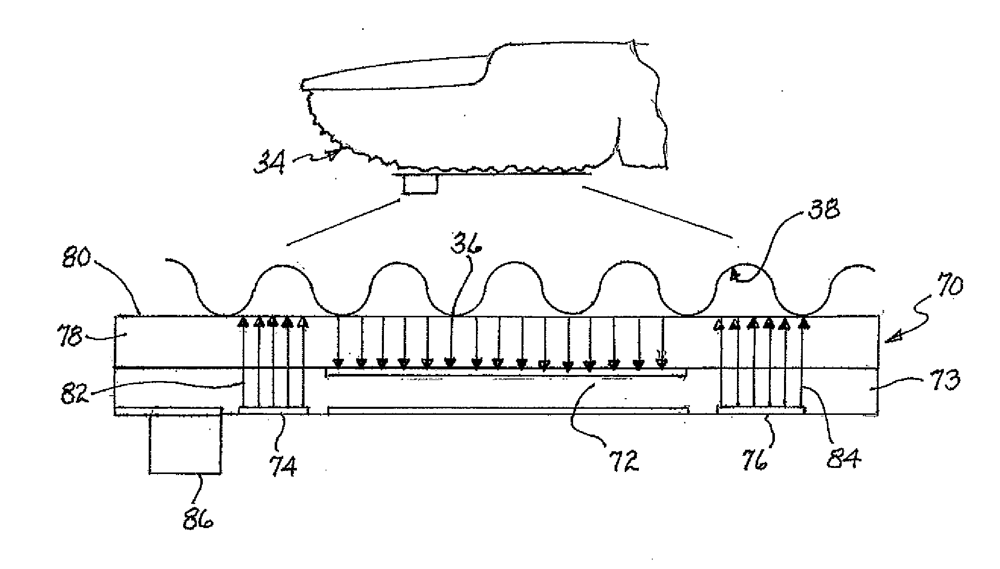
This patent describes a fingerprint sensor with multiple transmitter electrodes that are placed within the borders of the pixel array. These electrodes transmit a carrier signal for transmission into the user's fingertip, while neighboring electrodes are disabled to prevent unwanted signal coupling. The sensor also includes a demultiplexer to reduce the number of conductors that must extend between the pixel array and a related integrated circuit. Additionally, the sensor includes a cover layer for receiving a fingertip of a user, and the transmitter electrode is positioned close enough to the finger to allow for effective transmission of the carrier signal. These features improve the accuracy and simplicity of imaging fingerprints.

Problems solved by technology

The first type of fingerprint sensor described above results in a much higher-cost product, since the CMOS silicon chip in which the pixel array is formed must be at least the size of the fingerprint image required.
In the case of a touch sensor, or 2D sensor, this can require a relatively large area of silicon, measuring three-quarters of an inch square or larger, making it relatively costly.
On the other hand, the second type of fingerprint sensor described above, wherein metal traces are formed upon a non-semiconductor substrate, often develop an inferior signal due to the limitations on the widths of the lines used to transmit and receive the signal from which the fingerprint image is derived.
The smaller sizes of the transmitter and receivers, especially the transmitter, can also severely limit the thickness of material above the sensor.
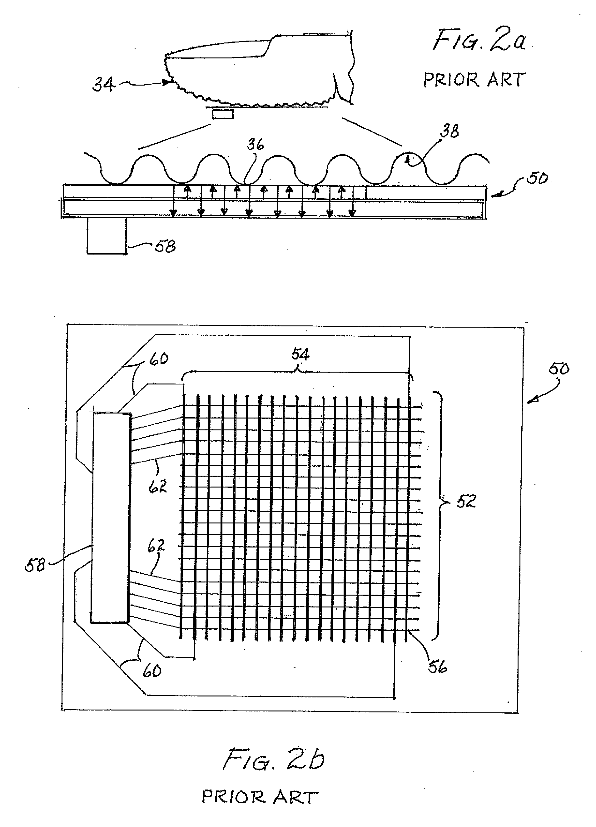
This method is extremely limited in signal strength because the column lines must be used as both transmission (Tx) lines and receiver (Rx) lines.
The use of the column line as both Tx (precharge) and Rx (receive, or read) severely limits the signal to noise capabilities that this method can produce.
In addition, this method is costly, as all of the column drivers must be designed to serve as both an output device (for normal display usage) and a highly sensitive input device (for fingerprint sensor usage).
However, as the receiver plate thickness is reduced, such fingerprint sensors are more easily damaged physically or mechanically because of the close proximity of the sensor surface to underlying electrical circuitry, thus reducing the durability and / or reliability of the sensor.
For example, conventional BGA-style fingerprint sensors, as well as newer, more advanced “flexible” fingerprint sensors, which enable a user to swipe a finger across a polyimide surface without directly contacting the sensor circuitry, are both susceptible to this type of damage.
Accordingly, for the second type of fingerprint sensor described above, the thickness and material type used to protect the fingerprint sensor is severely limited.
For example, a simple drop of a pen striking the exposed portion of the fingerprint sensor can damage the thin polyimide surface of the flexible fingerprint sensor, thus creating aesthetic defects and potentially damaging the sensor circuitry located just below the surface.
However, thicker protective coatings / surfaces introduce at least two new challenges: 1)—the signal strength from the signal transmitter, to the finger, then back to the receiver array, is greatly diminished as thickness of the cover increases, typically by the square of the increased distance (i.e., doubling the cover thickness reduces signal strength by a factor of four); and 2)—depending on how the transmitter signal is generated, the transmitter signal can be significantly de-focused as it travels from the transmitter to the receiver.
Moreover, as the thickness of the protective layer, separating the user's finger from the underlying signal sensing electrodes, is increased, the direct capacitive coupling of the radiated high frequency signal from the signal generating electrode to the array of signal sensing electrodes largely overwhelms any secondary coupling of the radiated high frequency signal through the user's finger.

Method used


Image

  • Apparatus and Method for TFT Fingerprint Sensor
  • Apparatus and Method for TFT Fingerprint Sensor
  • Apparatus and Method for TFT Fingerprint Sensor

Examples


Embodiment Construction

[0083]The following detailed description is to be read with reference to the figures, in which like elements in different figures have like reference numerals. The figures, which are not necessarily to scale, depict selected embodiments and are not intended to limit the scope of the invention.

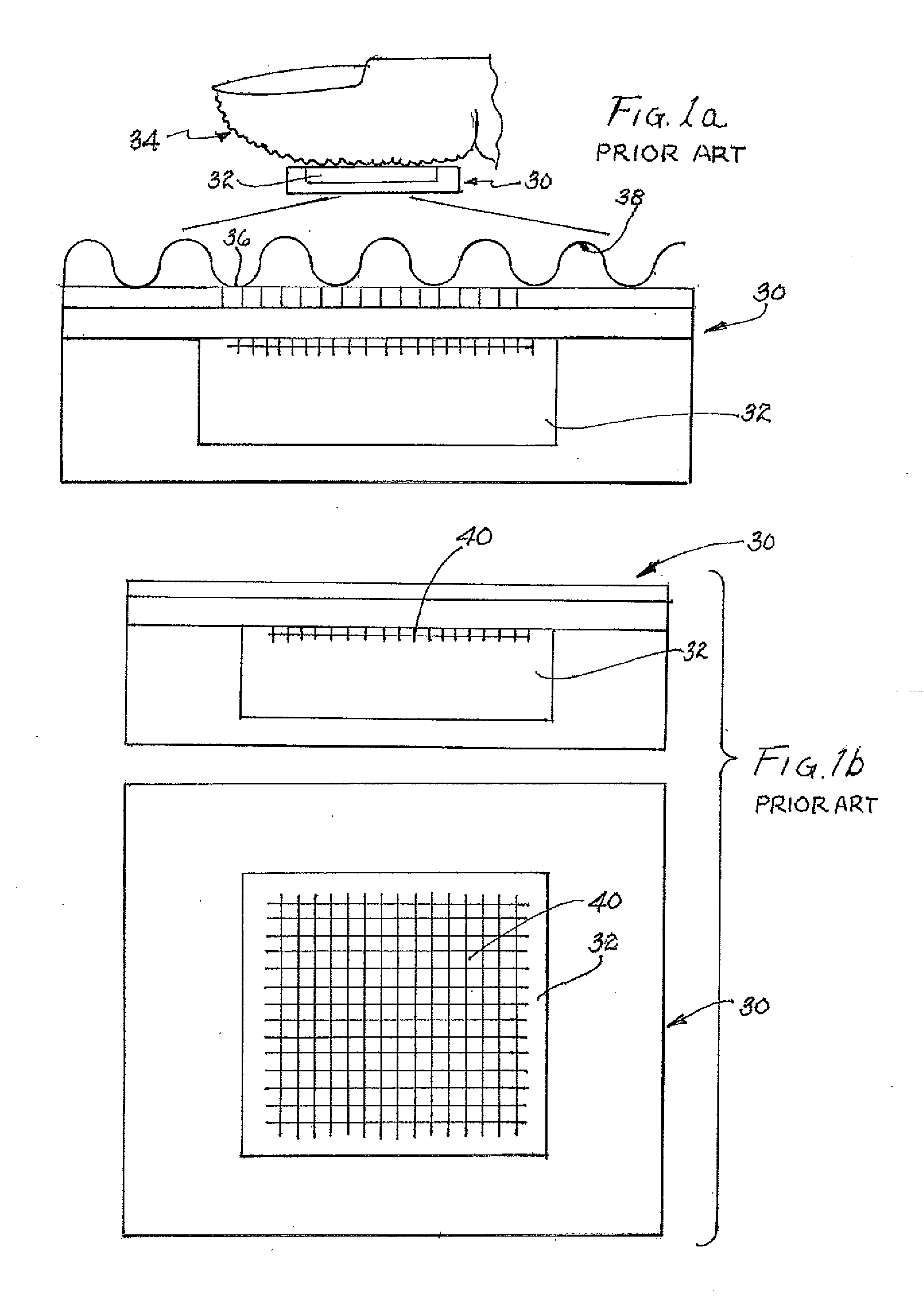
[0084]FIGS. 1a and 1b illustrate a known fingerprint sensor 30 which utilizes an entire silicon chip 32 as the receiver for signals derived from the user's fingertip 34. Various methods have been described for transmitting a signal into the user's finger, both on the silicon chip itself, and external to the silicon chip; in either case, the pixels 40 used to receive signals from the user's fingertip are directly formed on a silicon chip. The signal is received at each pixel in the silicon chip. Signal detection may be based upon voltage amplitude, signal phase shift, or other methods for detecting differences between signals that pass through a ridge 36 of the fingertip versus signals that pass...


PUM


Abstract

A low cost, two-dimensional, fingerprint sensor includes a pixel array, each pixel including a switch and a pixel electrode for forming a capacitance with a fingertip. One or more active transmission electrodes are spaced from a selected row of the pixel array, and transmit a carrier signal into the finger without direct coupling into the selected pixels. Signals sensed by the pixel array are coupled to an independent integrated circuit, and connections between the IC and the pixel array are reduced by demultiplexing row select lines, and by multiplexing sensed column data. Differential sensing may be used to improve common mode noise rejection. The fingerprint sensor may be conveniently incorporated within a conventional touchpad LCD panel, and can mimic the performance of lower density touchpad pixels.

Description

CROSS-REFERENCE TO RELATED APPLICATIONS[0001]This application claims the benefit of the earlier filing date of U.S. provisional patent application No. 61 / 820,477, filed on May 7, 2013, for “Apparatus and Method for TFT Fingerprint Sensor”, regarding all commonly-disclosed subject matter.BACKGROUND OF THE INVENTION[0002]1. Field of the Invention[0003]The present invention relates generally to electronic fingerprint sensors, and more particularly to a fingerprint sensor using a thin-film transistor (“TFT”) array to capacitively sense a user's fingerprint.[0004]2. Description of the Related Art[0005]Conventional fingerprint sensors currently being sourced to the commercial market use different methods for sensing a user's fingerprint. One type of fingerprint sensor includes a CMOS silicon chip having circuitry providing an arrayed multitude of “pixels”. The CMOS silicon chip is then coated with a protective coating that may be formed from a simple chemical coating, a flex substrate, or...

Claims


Application Information

Patent Timeline
Patent Type & Authority Applications(United States)
IPC IPC(8): G06F3/044G06V30/144
CPCG06F3/044G06F3/0446G06F3/041661G06V40/1306G06F2203/04111G06F2203/04103G06V30/144G06F2203/04102G06F3/041G06F3/0416
Inventor NELSON, RICHARD B.ERHART, RICHARD A.
Owner EGIS TECH
Learn More