AI technical title is built by Patsnap AI team. It summarizes the technical point description of the patent document.
a three-dimensional integrated circuit and circuit structure technology, applied in the field of forming circuitry, can solve the problems of increasing the cost of manufacturing equipment, 64-bit computer chips will need more devices, and laterally oriented devices consume significant chip area
Inactive Publication Date: 2011-02-15
BESANG
View PDF7 Cites 215 Cited by
Summary
Abstract
Description
Claims
Application Information
AI Technical Summary
This helps you quickly interpret patents by identifying the three key elements:
Problems solved by technology
Method used
Benefits of technology
Problems solved by technology
However, these laterally oriented devices consume significant amounts of chip area.
However, the 64-bit computer chip will need more devices since there are more bits to process at a given time.
The number of devices can be increased by making the devices included therein smaller, but this requires advances in lithography and increasingly expensive manufacturing equipment.
However, the yield of the computer chips fabricated in a run decreases as their area increases.
This increases the overall cost.
However, there are several problems with this.
One problem is that the masks used to fabricate the memory devices are not compatible with the masks used to fabricate the other electronic devices.
Hence, it is more complex and expensive to fabricate a computer chip with memory embedded in this way.
Another problem is that memory devices tend to be large and occupy a significant amount of area.
The total area of the computer chip can be increased, but as discussed above, this decreases the yield and increases the cost.
Method used
Image
Click on the blue label to locate the original text in one second.
Reading with bidirectional positioning of images and text.
Examples
Embodiment Construction
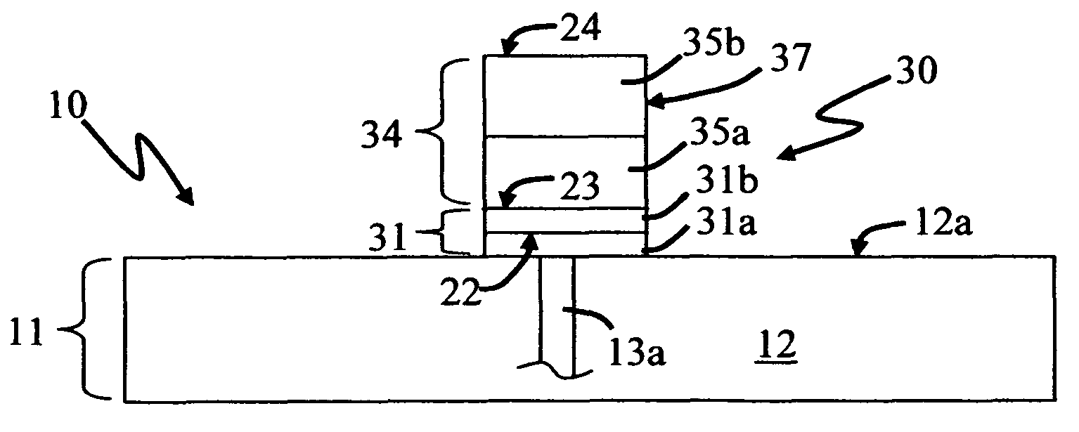
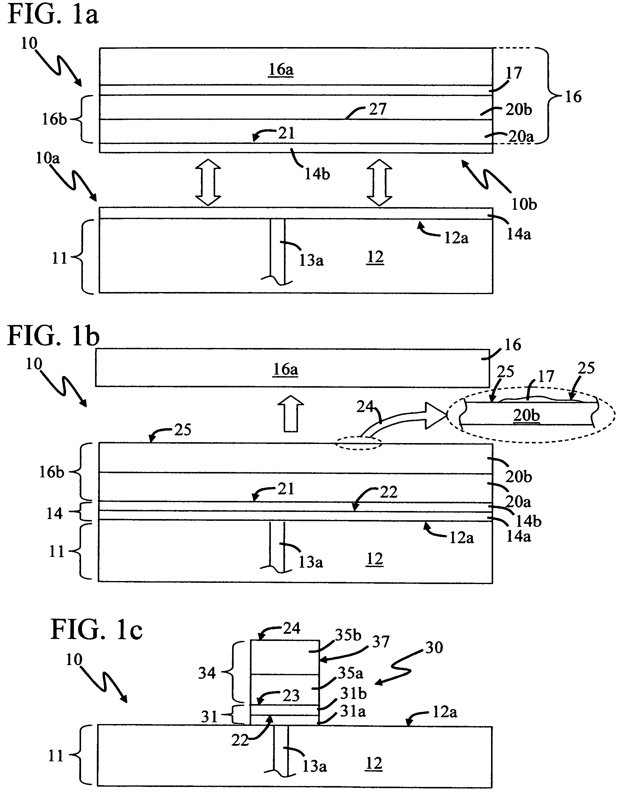
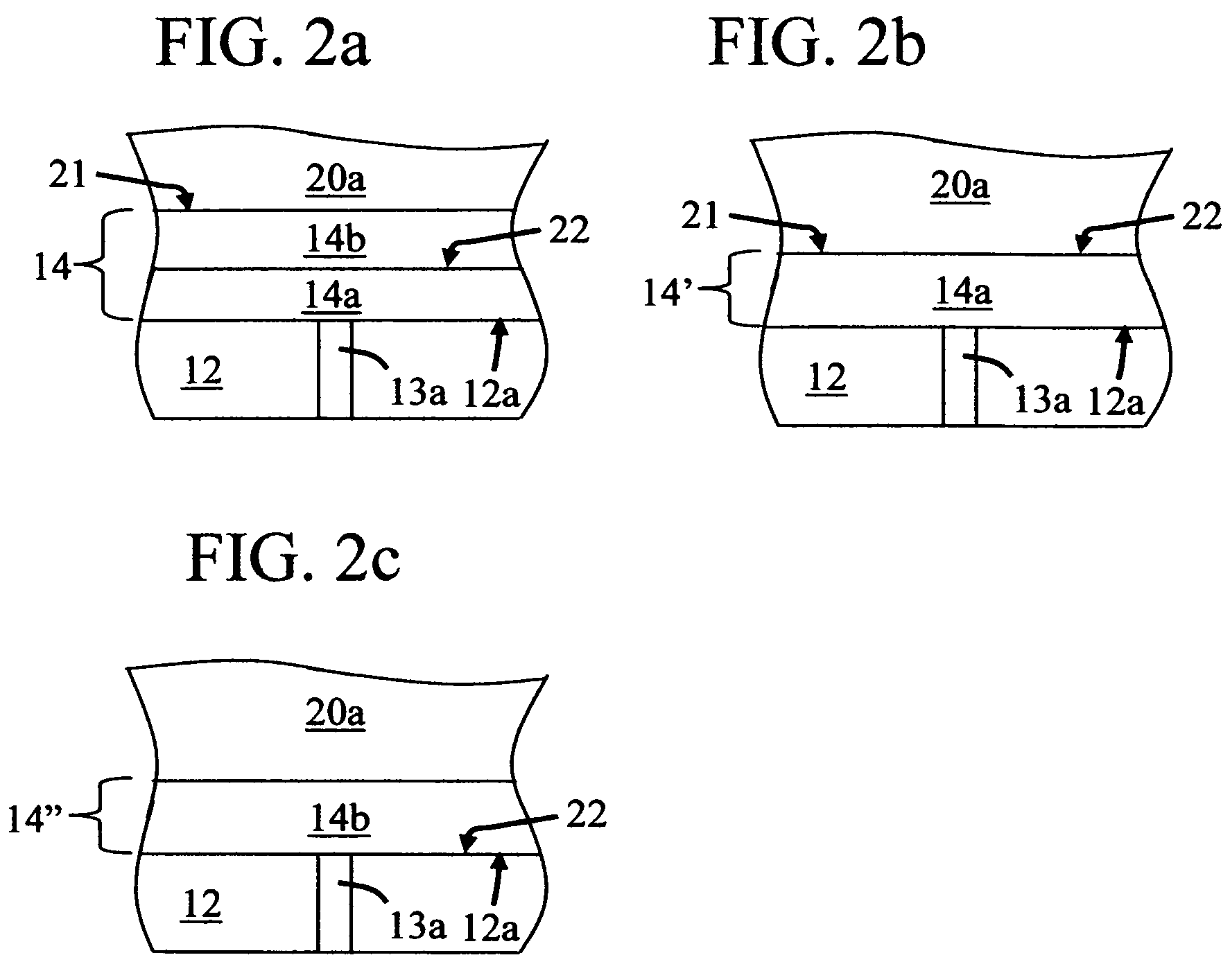
[0018]A semiconductor structure is disclosed for use with an electronic circuit in a computer chip. In accordance with the invention, the structure is bonded to an interconnect region and processed to form vertically oriented semiconductor devices that are positioned above the electronic circuit. The vertical devices are in communication with the electronic circuit through conductive lines extending through the interconnect region.
[0019]The invention provides several advantages, with one being that the vertical devices can replace corresponding lateral ones positioned on the same surface of the electronic circuit, as is usually done with cache memory. Replacing the horizontal devices with vertical ones is advantageous because this provides more area for the electronic circuit since the vertical devices are positioned above it instead of on the same surface. In this way, the electronic circuit can include more electronic devices without increasing the chip area. Further, more vertica...
PUM
Abstract
A semiconductor structure includes an interconnect region and a semiconductor stack bonded to the interconnect region through a bonding region. The stack includes at least two semiconductor layers having different electrical properties. The stack also includes single crystalline semiconductor material. The stack can be processed to form a mesa structure and the mesa structure can be processed to from a vertically oriented semiconductor device.
Description
[0001]This application is a continuation in part of U.S. patent application Ser. No. 11 / 378,059 filed on Mar. 17, 2006, which is a divisional of U.S. patent application Ser. No. 10 / 873,969 filed on Jun. 21, 2004, and is now U.S. Pat. No. 7,052,941, and claims the benefit of both prior applications. This application also claims benefit to prior U.S. patent application Ser. No. 10 / 934,270 filed on Sep. 3, 2004, Ser. No. 11 / 092,521 filed on Mar. 29, 2005, Ser. No. 11 / 092,501 filed on Mar. 29, 2005, Ser. No. 11 / 092,499 filed on Mar. 29, 2005, Ser. No. 11 / 092,500 filed on Mar. 29, 2005, Ser. No. 11 / 092,498 filed on Mar. 29, 2005, and Ser. No. 11 / 180,286 filed on Jul. 12, 2005. All of these applications are incorporated herein by reference.BACKGROUND OF THE INVENTION[0002]1. Field of the Invention[0003]The present invention relates generally to semiconductors and, more particularly, to forming circuitry using wafer bonding.[0004]2. Description of the Related Art[0005]Advances in semicondu...
Claims
Application Information
Patent Timeline
Application Date:The date an application was filed.
Publication Date:The date a patent or application was officially published.
First Publication Date:The earliest publication date of a patent with the same application number.
Issue Date:Publication date of the patent grant document.
PCT Entry Date:The Entry date of PCT National Phase.
Estimated Expiry Date:The statutory expiry date of a patent right according to the Patent Law, and it is the longest term of protection that the patent right can achieve without the termination of the patent right due to other reasons(Term extension factor has been taken into account ).
Invalid Date:Actual expiry date is based on effective date or publication date of legal transaction data of invalid patent.

