Multichip package leadframe including electrical bussing

Inactive Publication Date: 2011-03-08
MARVELL INT LTD
View PDF6 Cites 1 Cited by
  • Summary
  • Abstract
  • Description
  • Claims
  • Application Information

AI Technical Summary

Benefits of technology

[0017]In some embodiments, the system may comprise one of a group comprising a mobile phone, a laptop computer, a personal digital assistan

Problems solved by technology

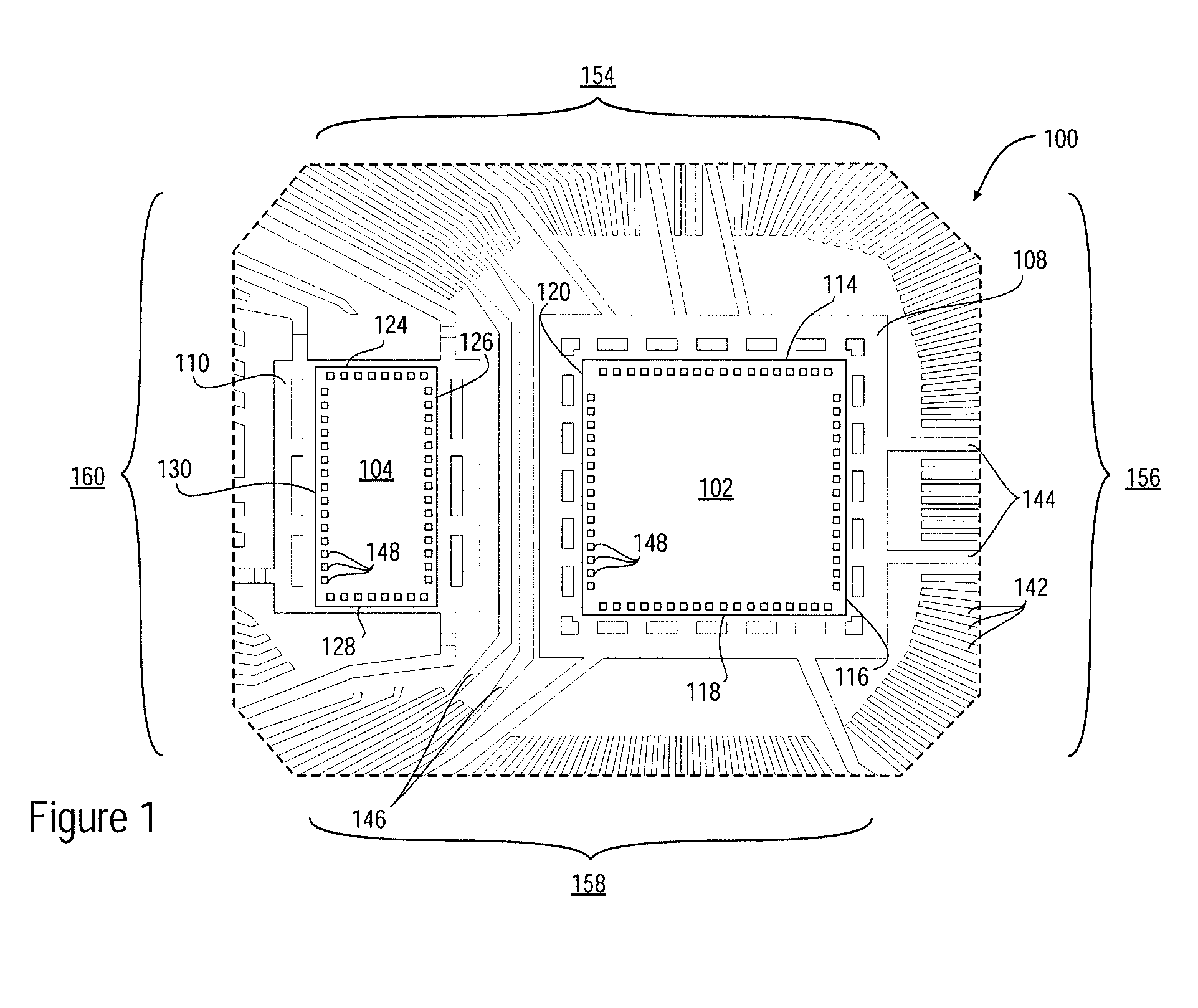
In multichip packages, wire bonding from those sides of a die that abut another die may be problematic.
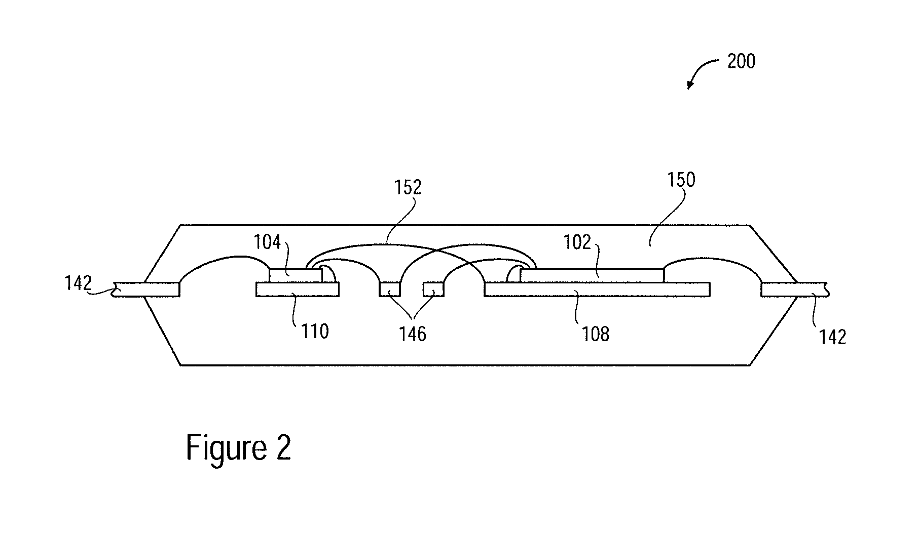
Long wires may result in shorting if wires were to touch during subsequent operations (e.g., during encapsulation).
Even if shorting were avoided, long wires may still be undesirable due to increased signal transmission time.
Unfortunately, this process is expensive, complex, and time-consuming.
This “solution,” however, simply adds cost, in terms of time and money, to packaging operations.

Method used


Image

  • Multichip package leadframe including electrical bussing
  • Multichip package leadframe including electrical bussing
  • Multichip package leadframe including electrical bussing

Examples


Embodiment Construction

[0025]In the following detailed description, reference is made to the accompanying drawings which form a part hereof wherein like numerals designate like parts throughout, and in which are illustrated by way of illustrative embodiments in which the invention may be practiced. It is to be understood that other embodiments may be utilized and structural or logical changes may be made without departing from the scope of the present invention. Therefore, the following detailed description is not to be taken in a limiting sense, and the scope of embodiments in accordance with the present invention is defined by the appended claims and their equivalents.

[0026]Various operations may be described as multiple discrete operations in turn, in a manner that may be helpful in understanding embodiments of the present invention; however, the order of description should not be construed to imply that these operations are order dependent.

[0027]For the purposes of the present invention, the phrase “A...


PUM


Abstract

Embodiments of the present invention provide electrical bussing for multichip leadframes. In various embodiments, a leadframe may comprise a first die paddle for receiving a first microelectronic device, a second die paddle for receiving a second microelectronic device, and at least one electrical bus disposed between the first die paddle and the second die paddle. In various ones of these embodiments, the electrical bus may be configured to supply a potential to at least one of the first and second microelectronic devices.

Description

CROSS REFERENCE TO RELATED APPLICATIONS[0001]The present application claims priority to U.S. Provisional Patent Application No. 60 / 822,439, filed Aug. 15, 2006, entitled “LEADED MULTICHIP PACKAGE LEADFRAME EMPLOYING MULTIPLE BUS STRIPS BETWEEN ELECTRICALLY ISOLATED DIE PADDLES,” the entire disclosure of which is hereby incorporated by reference in its entirety.TECHNICAL FIELD[0002]Embodiments of the present invention relate to the field of integrated circuits, and more particularly, to multichip electronic packages and leadframes.BACKGROUND[0003]In the current state of integrated circuit technology, an integrated circuit device will often be in the form of a die. Such a die will typically be mounted onto an underlying substrate such as a carrier substrate to form a “package.” For example, some packages will include one or more dies coupled to a substrate such as a leadframe, which is frequently made of copper or copper alloy material, and may include a die paddle to support the die....

Claims


Application Information

Patent Timeline
IPC IPC(8): H01L23/52
CPCH01L23/49503H01L23/49541H01L23/49575H01L2224/48091H01L2224/48247H01L2924/30107H01L24/48H01L2924/00014H01L2924/00H01L2924/14H01L2924/181H01L2224/05554H01L2924/00012H01L2224/45099H01L2224/45015H01L2924/207
Inventor CUSACK, MICHAEL D.
Owner MARVELL INT LTD
Why Eureka
Try Eureka